Characterization of atomic-layer MoS2 synthesized using a hot filament chemical vapor deposition method
Peng Ying-Zi1, 2, †,  , Song Yang1, Xie Xiao-Qiang1, Li Yuan1, 2, Qian Zheng-Hong2, Bai Ru2
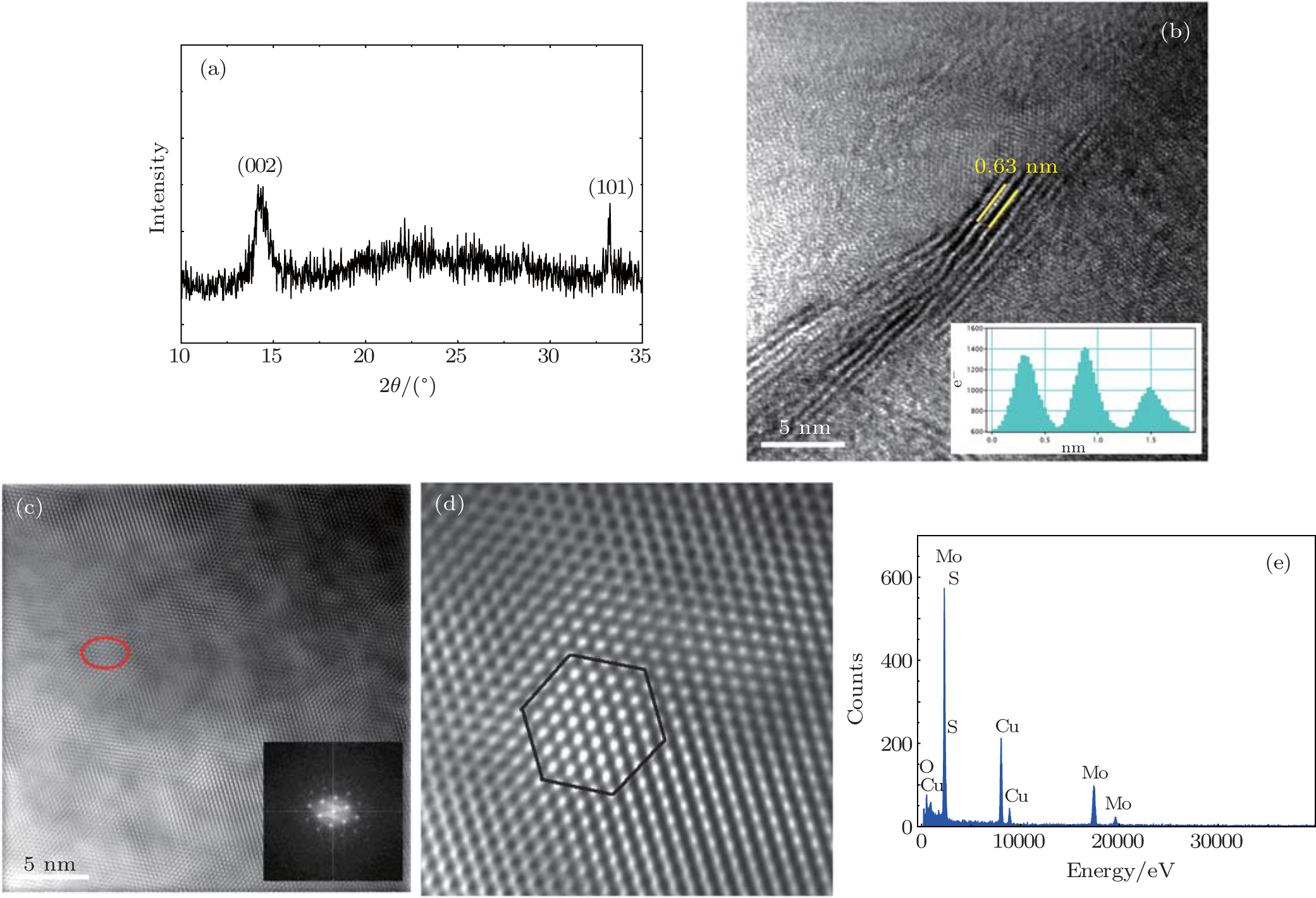
, Song Yang1, Xie Xiao-Qiang1, Li Yuan1, 2, Qian Zheng-Hong2, Bai Ru2 (a) A typical XRD pattern for the MoS2 thin film. (b)–(d) HRTEM images of the atomic-layer MoS2 films showing the atomic layers of the MoS2 films and the corresponding EDS spectrum from the region enclosed by the circle of selected area (e). The inset in panel (b) shows the corresponding profile revealing the distance of the interlayer. The inset in panel (c) reveals the corresponding FFT of the HRTEM image. Panel (d) shows the large image of the corresponding area enclosed by the circle in panel (c).