


Preparation and room temperature NO2-sensing performances of porous silicon/V2O5 nanorods
[Yan Wen-Jun, Hu Ming, Liang Ji-Ran, Wang Deng-Feng, Wei Yu-Long, Qin Yu-Xiang†,  ]
]
]
|
|


† Corresponding author. E-mail:
Project supported by the National Natural Science Foundation of China (Grant Nos. 61271070, 61274074, and 61574100).
In this paper, porous silicon/V2O5 nanorod composites are prepared by a heating process of as-sputtered V film on porous silicon (PS) at 600 °C for different times (15, 30, and 45 min) in air. The morphologies and crystal structures of the samples are investigated by field emission scanning electron microscope (FESEM), x-ray diffractometer (XRD), x-ray photoelectron spectroscopy (XPS), and Raman spectrum (RS). An improved understanding of the growth process of V2O5 nanorods on PS is presented. The gas sensing properties of samples are measured for NO2 gas of 0.25 ppm∼3 ppm at 25 °C. We investigate the effects of the annealing time on the NO2-sensing performances of the samples. The sample obtained at 600 °C for 30 min exhibits a very strong response and fast response-recovery rate to ppm level NO2, indicating a p-type semiconducting behavior. The XPS analysis reveals that the heating process for 30 min produces the biggest number of oxygen vacancies in the nanorods, which is highly beneficial to gas sensing. The significant NO2 sensing performance of the sample obtained at 600 °C for 30 min probably is due to the strong amplification effect of the heterojunction between PS and V2O5 and a large number of oxygen vacancies in the nanorods.
Today, NO2 sensor is the need of the hour that could have high sensitivity and low operating temperature at low concentrations. Solid-state resistive-type gas sensors based on one-dimensional metal oxide semiconductors (1D MOS) with large surface-to-volume ratios, have been widely used for sensing NO2 gas.[1–4] Despite the promising potential of 1D MOS for NO2 gas sensor applications, some aspects such as improvement of sensitivity, low selectivity and high operating temperature are persistent challenges to their actual implementation. Many recent studies have shown that the important sensing parameters of 1D MOS sensors can be improved by making the composite with others,[5] e.g., noble metals,[6–8] dissimilar metal oxides,[9–14] organics,[15] and other semiconductors.[16–19]
As two kinds of important semiconductors, V2O5 and porous silicon (PS) have gained more and more attention over the past decade.[20–22] V2O5 offers the possibility to be a reliable sensing material due to its layered crystal structure. To date, 1D V2O5 nanostructures have been used for detecting gases such as ethanol[23,24] and ammonia.[25,26] However, there are rare reports about V2O5 based NO2 sensors. Yu et al.[27] reported V2O5 nanotubes response to both ethanol vapor and NO2 gases at 80 °C. This sensor has two shortcomings including poor selectivity between gases and relatively high operating temperature (e.g. 80 °C).
PS has been used extensively for detecting NO2 at low temperatures due to its large specific surface area and high chemical reactivity.[20,28] However, the instability of gas-sensitivity and lack of thermal stability restrict the commercial applications of PS. A gas sensor based on composites of PS and low-dimensional nanomaterials may be beneficial for enhancing gas response properties for their synergetic enhancement or heterojunction effects. There are rare reports about the gas sensing properties of PS and metal oxide nanostructures (ZnO, WO3, etc.).[29–31] The special composites exhibit a significant improvement on gas sensing performances with respect to the monocomponent, therefore the heterojunction barrier-controlled sensing mechanism is proposed. In our previous work, the high sensitivity and selectivity of the PS/V2O5 nanorods to NO2 gas at room temperature were reported, but no detailed study on the growth mechanism of the nanorods on PS nor the effect of the synthesis process on its NO2-sensing performance was conducted.
In the present work, the PS/V2O5 composite is prepared by a very simple non-catalytic one-step process of directly annealing PS/V film. We describe the growth process of the V2O5 nanorods synthesized from V film on the PS substrate. The effects of heat treatment on the microstructure and gas sensing properties of the samples are investigated. Field emission scanning electron microscope (FESEM) is used to study the surface morphology. The crystalline properties and phases are determined by an x-ray diffractometer (XRD) and Raman analysis. X-ray photoelectron spectroscopy (XPS) is used to determine the chemical composition of the samples.
PS was prepared by the galvanostatic electrochemical etching of p-type monocrystalline silicon (100) wafer (resistivity 10 Ω·cm–15 Ω·cm). The electrolyte was a mixture of 40 wt% HF and 99.5 wt% N, N-dimethyl formamide with 1:2 volume ratio. The anodization was performed for 8 min with an etching current density of 100 mA/cm2 as described in our previous work.[32] The average pore size of the obtained PS is ∼ 1.2 μm in diameter and 12 μm in depth. The porosity of the porous layer is 39%–42%.
The V2O5 nanorods on PS were prepared through magnetron sputtering followed by annealing as described in our previous work.[33] Firstly, a V film with a thickness of ∼ 300 nm was deposited on PS by DC magnetron sputtering. The sputtering conditions were as follows: 2 mm in diameter, 3-mm thick V target (purity 99.999%); input power of 135 W; chamber atmosphere of 2-Pa Ar; deposition carried out for 40 min. The V-deposited PSs were subsequently annealed in air at 300, 400, 500, and 600 °C for different times (15, 30, and 45 min) in a standard program-controlled furnace with a heating rate of 5 °C/min. After the annealing process, the samples were cooled down inside the furnace to make the V2O5 nanorods suitably crystallized and stabilized. As a result, different V2O5 nanostructures were obtained on PSs.
The different V2O5 nanostructures formed on PSs were analyzed by using various characterization techniques. FESEM (FEI Nanosem 430) and transmission electron microscopy (TEM, Tecnai G2 F20) were employed to examine microstructures. XRD (D/MAX 2500) with Cu Kα radiation was used to investigate the phases and crystalline structures of samples. XPS (Perkin elemer PHI-1600 ESCA System) with a Mg Kα excitation source was used to characterize the surface elemental composition distribution profile and chemical state. Raman spectrum (RS) (Thermo Scientific confocal DXR Raman microscope) with a 532-nm wavelength Nd:YAG laser was used to characterize the bond configuration.
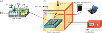
The gas sensing properties of PS/V2O5 composites were evaluated in a static gas sensing characterization system consisting of a glass test chamber, a flat heating plate, a programmable digital multimeter and data acquisition system.[34] In order to realize the electrically ohmic connection between the sensor and the digital multimeter, two ∼ 120-nm-thick Pt film electrodes were deposited onto the surface of the PS/V2O5 composite by magnetron sputtering. Figures
 | Fig. 1. Schematic diagram of (a) the resistive-type nanocomposite gas sensor and (b) the gas sensing measurement system. |
Figure
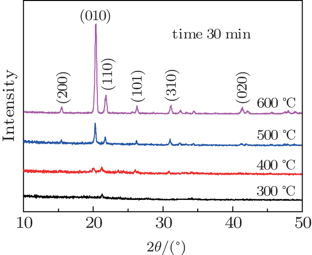 | Fig. 2. XRD patterns of V2O5 products on PS synthesized at different temperatures for 30 min. |
Figures
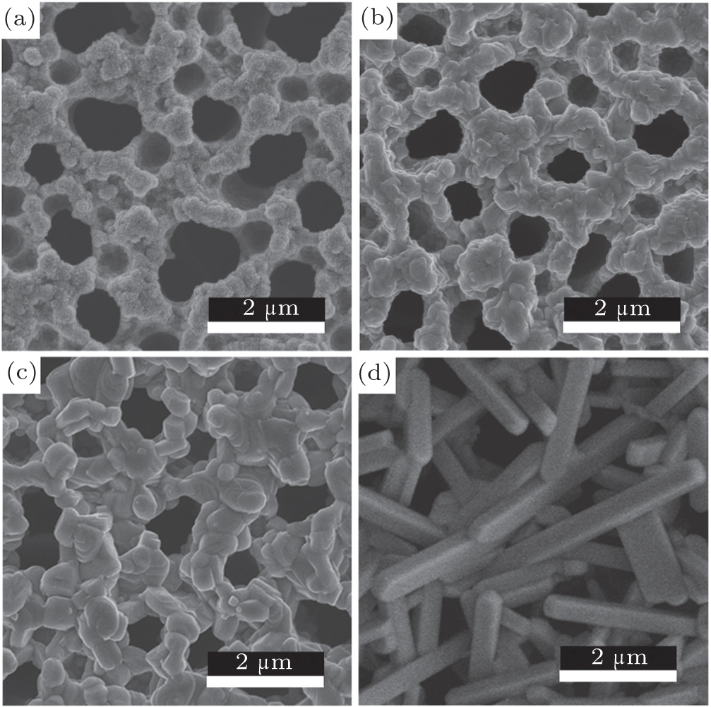 | Fig. 3. SEM images of (a) the as-deposited V film with 300 nm in thickness on the PS surface, and annealed samples for 30 min at (b) 400 °C, (c) 500 °C, and (d) 600 °C respectively. |
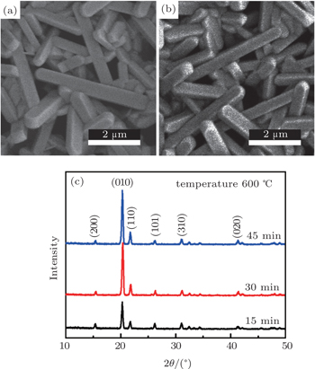
In order to investigate the synthesis process of the V2O5 nanorods on PS deeply, we anneal the as-deposited V film on PS at 600 °C for different times (15, 30, and 45 min) in air atmosphere. The surface morphologies and XRD patterns of the samples annealed at 600 °C for different times are shown in Figs.
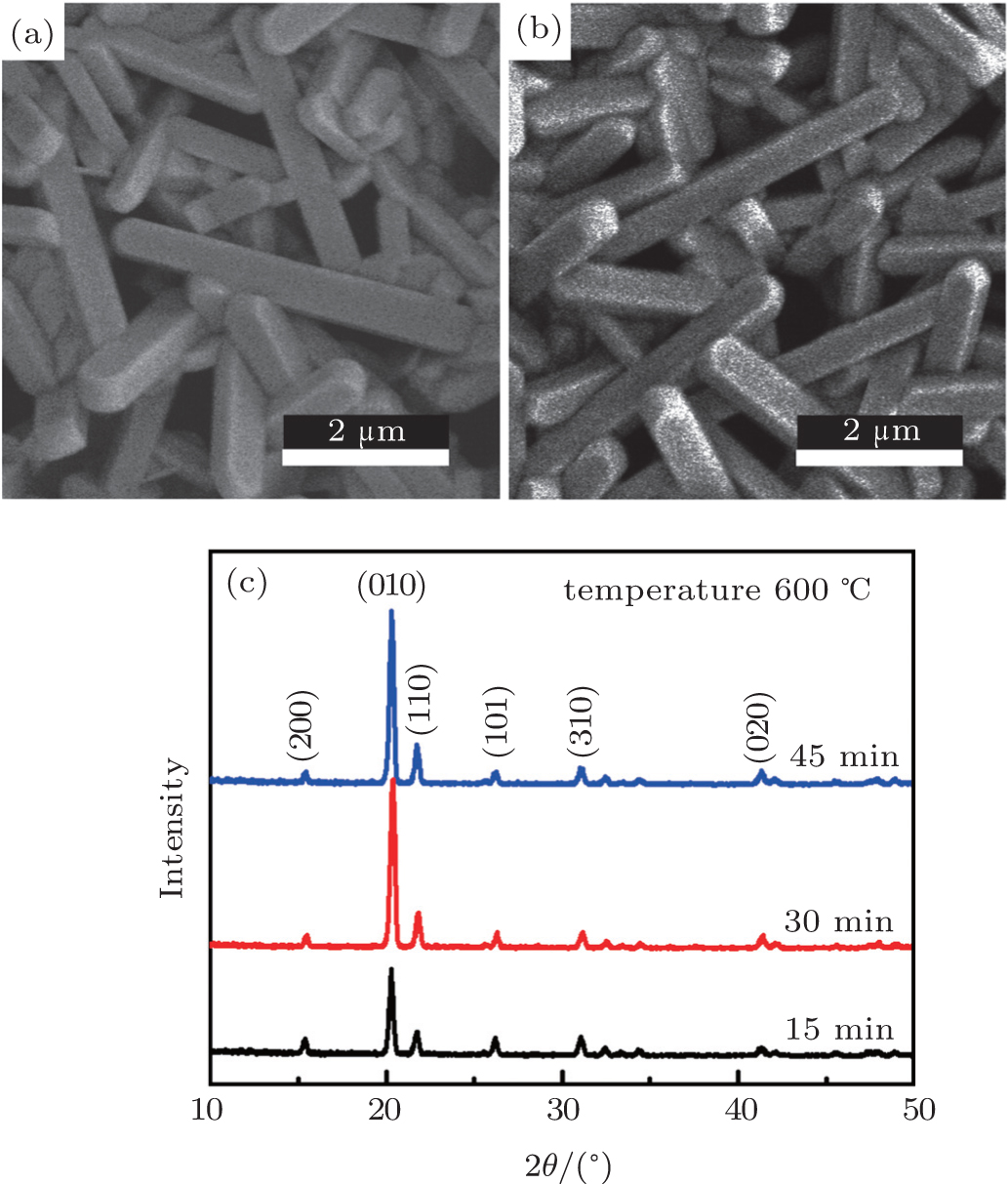 | Fig. 4. SEM images of PS/V2O5 nanorods annealed at 600 °C for (a) 15 min and (b) 45 min. (c) XRD patterns of V2O5 nanorods synthesized at 600 °C for different times. |
The microstructures of V2O5 nanorods annealed at 600 °C are further confirmed using XPS. Figures
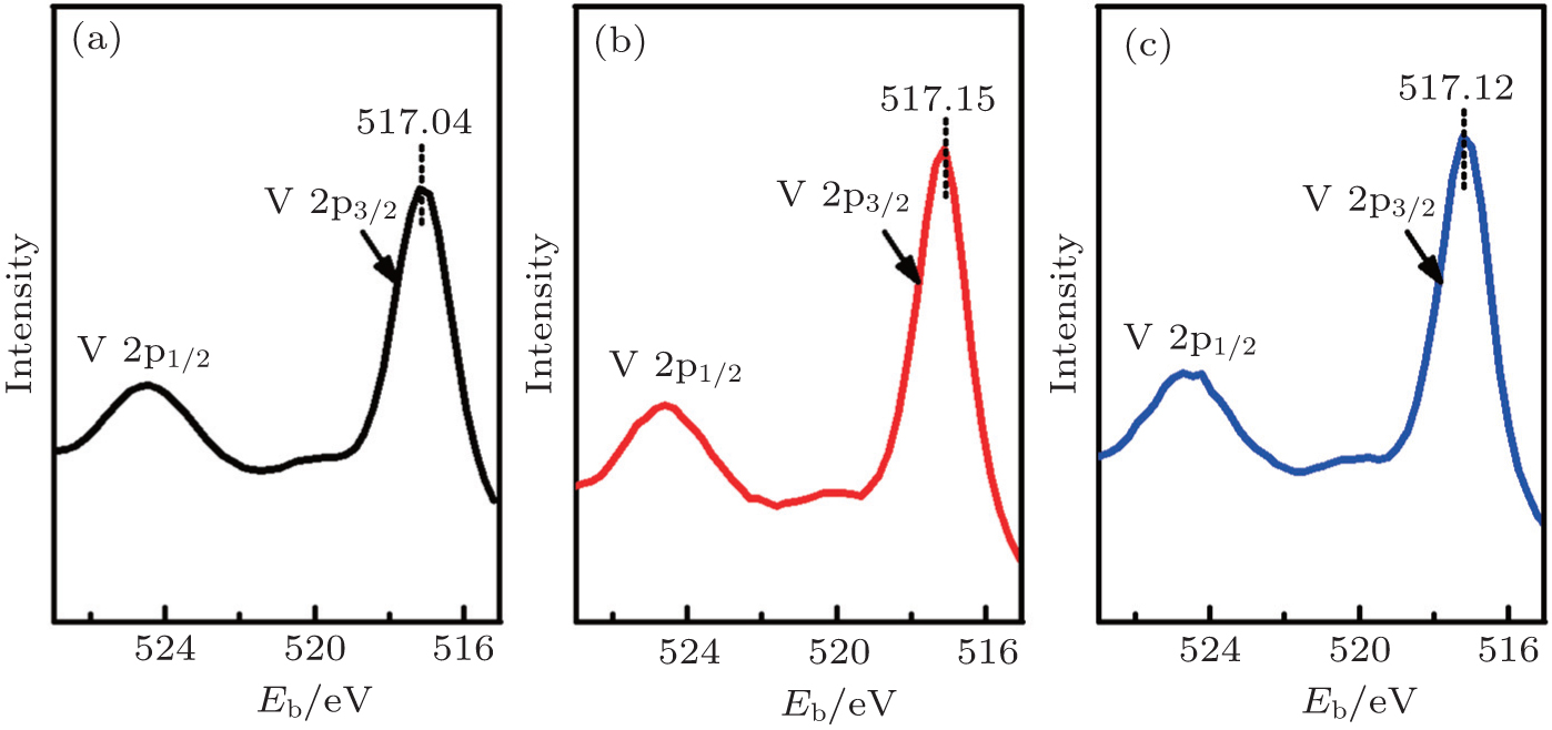 | Fig. 5. High resolution XPS core level V 2p spectra of PS/V2O5 nanorods annealed at 600 °C for (a) 15 min, (b) 30 min, and (c) 45 min. |
To further investigate the microstructure of PS/V2O5 nanorods at 600 °C for 30 min, the RS is measured, which is shown in Fig.
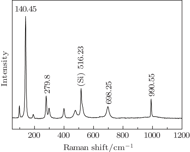 | Fig. 6. Raman spectrum of PS/V2O5 nanorods annealed at 600 °C for 30 min. |
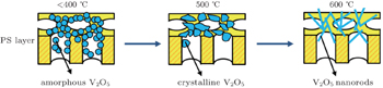
Through analyzing the morphological and structural characteristics of V2O5 nanorods grown on PS, we try to explain the growth mechanism of the nanorods. We suppose that the process of V2O5 nanorods is related to the surface morphology of the substrate PS and the annealing temperature. Boston et al.[41] indicated that sites on the rough surface of the porous matrix act as microcrucibles and thus provide an insight into the mechanism that drive metal oxide nanowire growth at high temperatures. According to the result of Zou et al.,[36] after annealing in oxygen ambience, the as-sputtered amorphous V2O5 films on glass substrates dramatically transform into V2O5 nanorods and large V2O5 particles on Si substrate, because on the glass, the as-prepared V2O5 shows a textured surface, while the as-prepared film on Si is much smoother.
Here, V granular film deposited on PS reacts with O2 in air ambience with furnace temperature increasing. But the post annealing treatment below 400 °C does not provide enough energy to form a crystal structure, resulting in the amorphous V2O5. The next crystallization process of amorphous V2O5 is sensitive to the temperature in a range from 400 °C to 500 °C. Furthermore, the rough surface of the substrate PS can act as the nucleation site to benefit the growth of V2O5 nanorods, and the thermodynamic-related surface diffusion controls the process at high temperatures. Ultimately, the initial V film transforms into V2O5 nanorods completely after annealing at 600 °C. The crystallization process is illustrated in Fig.
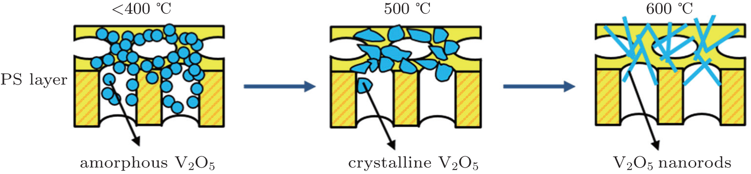 | Fig. 7. Schematic drawing of the formation process of V2O5 nanorods. |
As reported in our previous work, the optimum operating temperature of PS/V2O5 nanorods is 25 °C.[33] Thus the subsequent gas sensing measurements are carried out at 25 °C.
Figure
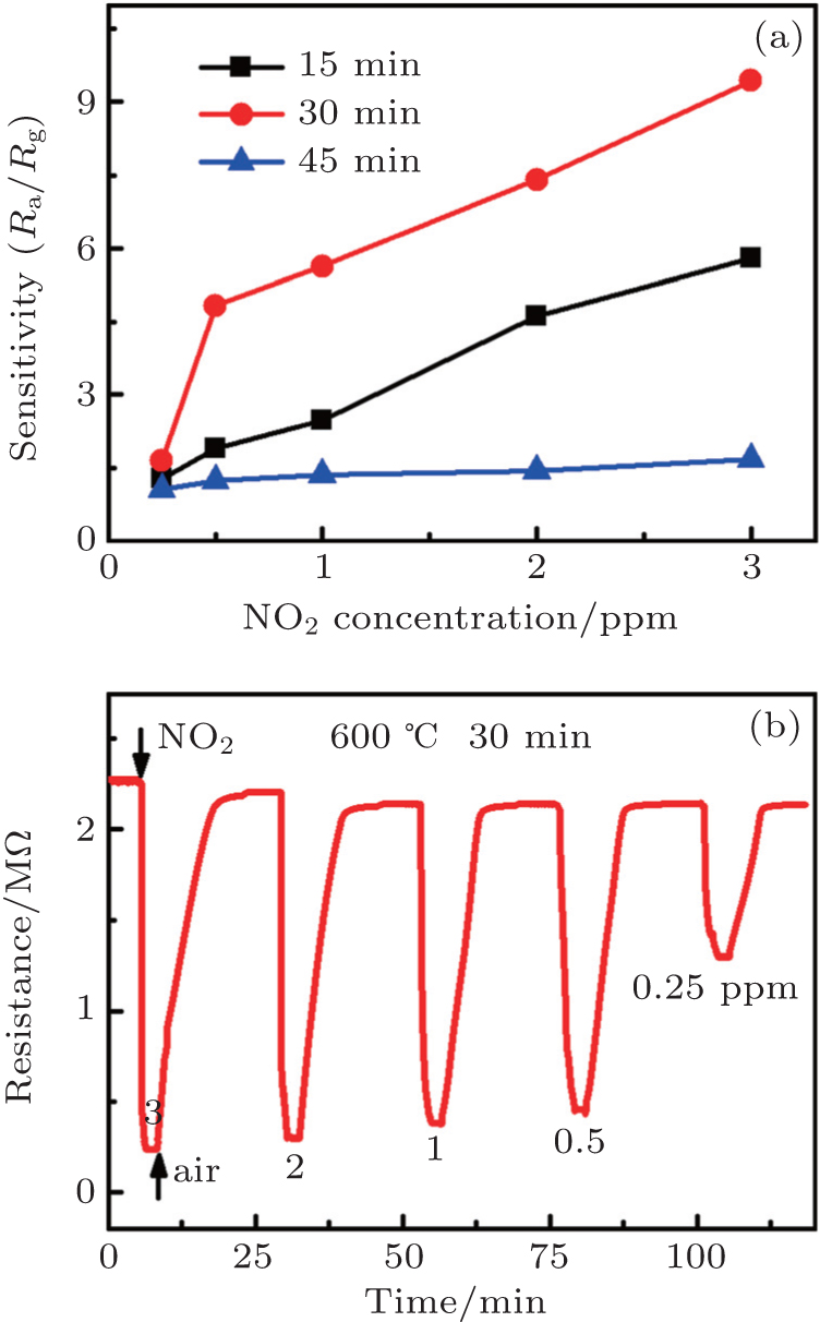 | Fig. 8. (a) NO2 concentration-dependent response values of PS/V2O5 nanorods at 25 °C. (b) Dynamic response curve of PS/V2O5 nanorods annealed at 600 °C for 30 min to various concentrations of NO2 at 25 °C. |
Figure
Furthermore, listed in Table
| Table 1. Comparisons of the response, NO2 testing concentration and operating temperature between the PS/V2O5 nanorods and other V2O5 sensors. . |
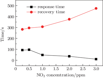
The response time and recovery time of the PS/V2O5 nanorods synthesized at 600 °C for 30 min each as a function of NO2 concentration is shown in Fig.
 | Fig. 9. Variations of response time and recovery time of the PS/V2O5 nanorods synthesized at 600 °C for 30 min with NO2 concentration. |
Since V2O5 behaves as an n-type semiconductor in gas sensing which is controlled by the surface conductance, the hetero-structure (p-PS/n-V2O5) is formed at the interface between them. In the hetero-structure, a depletion layer and the associated potential barrier exist. Both the PS and V2O5 nanorods can result in a specially large density of oxygen vacancy defects and dangling bonds, which makes the surface of the PS/V2O5 composite much more active in absorbing oxygen. The enhanced oxygen molecules adsorbed on the surface capture more free electrons from the conducting band. As a result, the depletion region is increased and the band bending is further, leading to an inversion layer instead of a depletion layer and indicating a p-type semiconductor property. As observed in XPS analysis, the sample synthesized at 600 °C for 30 min attains the maximal number of oxygen vacancies on the surface, leading to its greatest response to NO2.
A composite of PS/V2O5 nanorods is fabricated by an efficient non-catalytic method based on heating sputtering-deposited pure V film on PS in air at 600 °C. The process of the V2O5 nanorods growth on PS is investigated. The rough surface of the substrate PS acts as the nucleation sites to benefit the growth of V2O5 nanorods, and the thermodynamic-related surface diffusion controls the process at high temperatures. Oxygen vacancies are introduced into the composite structure in the annealing process. All the samples indicate a p-type conductive sensing behavior to NO2 gas at 25 °C. However, the sample annealed at 600 °C for 30 min shows the strongest response to ppm level NO2 with a fast response-recovery rate, owing to its improved crystallinity and significant oxygen vacancies.
| 1 | |
| 2 | |
| 3 | |
| 4 | |
| 5 | |
| 6 | |
| 7 | |
| 8 | |
| 9 | |
| 10 | |
| 11 | |
| 12 | |
| 13 | |
| 14 | |
| 15 | |
| 16 | |
| 17 | |
| 18 | |
| 19 | |
| 20 | |
| 21 | |
| 22 | |
| 23 | |
| 24 | |
| 25 | |
| 26 | |
| 27 | |
| 28 | |
| 29 | |
| 30 | |
| 31 | |
| 32 | |
| 33 | |
| 34 | |
| 35 | |
| 36 | |
| 37 | |
| 38 | |
| 39 | |
| 40 | |
| 41 | |
| 42 | |
| 43 | |
| 44 |