Performance improvement of AlGaN-based deep ultraviolet light-emitting diodes with double electron blocking layers
Laboratory of Nanophotonic Functional Materials and Devices, Institute of Opto-Electronic Materials and Technology, South China Normal University, Guangzhou 510631, China
† Corresponding author. E-mail: sunhq@scnu.edu.cn
Project supported by the Special Strategic Emerging Industries of Guangdong Province, China (Grant No. 2012A080304006), the Major Scientific and Technological Projects of Zhongshan City, Guangdong Province, China (Grant No. 2014A2FC204), and the Forefront of Technology Innovation and Key Technology Projects of Guangdong Province, China (Grant Nos. 2014B010121001 and 2014B010119004).
1. IntroductionOver the past decades, plenty of studies have focused on the performance optimizations of laser diodes (LDs) and visible high-brightness light-emitting diodes (LEDs) theoretically and experimentally,[1–3] especially the organic LEDs,[4,5] and GaN-based blue LEDs,[6,7] and very recently some new achievements have also be reported in this field.[8–11] In order to enhance the internal quantum efficiency (IQE) as well as reduce efficiency droop, many researches focus on improving light output power and increasing radioactive recombination by increasing hole injection, strengthening carrier confinement in the quantum wells (QWs), alleviating electron leakage and weakening polarization electrostatic field in the active region.[12,13] All of those efforts lead to entering the mature period of visible light emission device technologies. Therefore, a new field-invisible light optoelectronic device with a shorter wavelength, known as an ultraviolet light-emitting diode (UV-LED), has gained researchers’ close attention. The reasons can be attributed to their extensive roles in science research and daily life, such as chemical sensors, medical applications, water sterilization, full-color displays, etc.[14–16]
Despite the attractive prospect, there are also several challenges to the AlGaN-based UV-LED, such as poor hole injection efficiency and electron leakage from multi-quantum wells (MQWs) into the p-type layers, which leads to low carrier concentrations in active layers and weak radioactive recombination.[17,18] In recent years, various approaches have been put forward to cope with those challenges. Such as replacing conventional electron blocking layer (EBL) with multi-quantum-barrier EBL[19] to improve the electron injection efficiency, adapting composition-varying AlGaN multilayer barriers in the multiple quantum wells (MQWs)[20] to improve the performance of AlGaN-based UV-LED, and using a p-GaN micro-rod technique to improve the light output power of near-UV InGaN/AlGaN LED.[21] The reasons can be explained as follows. The markedly reduced polarization-induced electrostatic field within QWs suppresses the electron leakage and increases the hole injection efficiency; as a result, more electrons can recombine with holes. Wu et al.[22] reported that the hole injection efficiency of AlGaN-based deep UV-LEDs can be enhanced markedly when a single step quantum well is adapted to the EBL, resulting from the alleviated band bending near the special EBL. Zhang et al. have proposed that a p-AlGaN inserted layer with lower Al composition than that of the last barrier between the EBL and active region in AlGaN-based UV-LEDs can also enhance hole injection and lower the electron leakage tremendously.[23] On the other hand, some suggestions about designing the EBL have also been reported, such as AlGaN-based deep UV-LED with Al content-graded AlGaN EBL,[24] near–UV LED with InAlN/GaN superlattice EBL,[25] AlGaN/GaN superlattice EBL,[26] and adopting n-AlGaN EBL.[27] All of those methods reach a similar purpose of enhancing carrier inject efficiency, reducing electron leakage, and finally improving radioactive recombination, IQE, and output power. However, those complicated structures are hard to grow in practice.
Recently, a novel structure of blue GaN-based LED with double EBLs to mitigate the efficiency droop at a high current density was proposed.[28] What they adopted is p-AlGaN EBL and p-AlInGaN EBL with a p-GaN layer inserted between them near the p-side region. In addition, the simulations in Refs. [29] and [30] also indicate the advantage of the n-AlGaN EBL over the p-AlGaN EBL in GaN-based blue LED, and according to Ding et al., a specially designed n-AlGaN hole blocking layer is also beneficial to improving the performance of blue InGaN LED.[31] Inspired by their ideas, in this work, on the basis of a conventional UV-LED with a high Al component p-AlGaN EBL, we propose a novel structure, that is, AlGaN-based deep UV LEDs with double EBLs on both sides of the active region to enhance the hole and electron injection efficiency. Meanwhile, we make use of the crosslight advance physical model of the semiconductor device (APSYS) program to probe into the band diagram, and the optical and electrical properties of the structure. APSYS is a general purpose 2D/3D modeling software program for semiconductor devices. Based on the carrier transport equations, the Schrödinger equation, the current-continuity equation self-consistently and Poisson's equation,[32] it includes many advanced physical models such as hot carrier transport, hetero junction models, and thermal analysis. The basic physical models are described as follows:

where
Jn =
nμn∇
Efn and
Jp =
pμp∇
Efp denote the densities of electrons and holes;
μn and
μp denote the electron mobility and hole mobility;
Efn and
Efp denote the quasi-Fermi levels of electron and hole;

,
Rsp,
Rst,
Rau, and
Gopt(
t) denote the
j-th SRH deep level trap recombination rate, spontaneous radiative recombination rate, stimulated radiative recombination rate, Auger recombination rate, and light generation rate, respectively;
fD and
fA are the probabilities of electrons occupying benefactor and hole acceptor impurity; ∇
V is the electric field;
εdc is the relative dielectric constant;
n and
p are the electron and hole concentration respectively;
NA is the shallow donor doping concentration;
ND is the acceptor doping concentration;
Ntj is the
j-th SRH density of deep level traps;
ftj is the probability of electrons occupying the
j-th deep level trap; and
δ = 1 means donor and
δ = 0 means acceptor.
The non-radiative recombination process contains the indirect recombination (Shockley–Read–Hall [SRH] recombination) and Auger recombination. The SRH recombination is given as

where
n1j and
p1j are the carrier concentrations for electrons and holes, when electron and hole quasi-Fermi level merge into an energy level in the
J trap.
cnj and
cpj are the carrier trapping coefficients.
Auger recombination is given as

where
Cn and
Cp are constants of the special material, denoting the auger recombination coefficients for electron and hole, respectively;
ni is the intrinsic carrier density.
The carrier concentrations in the semiconductor device are described by the Fermi–Dirac distribution and parabolic state density:
where
F1/2 is half of the Fermi integral. More detailed physical models can be found in the APSYS manual provided by the Crosslight Company.
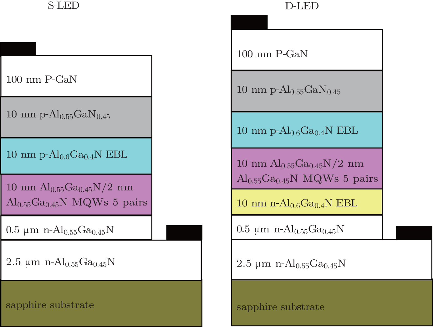
2. LED structures and simulation parametersThe conventional structure UV-LED with a single p-AlGaN EBL in the p-side, denoted as S-LED, which is viewed as a reference, is shown in Fig. 1. The redesigned structure UV-LED with double EBLs that are p-AlGaN EBL near the p-side and n-AlGaN EBL near the n-side, respectively, is denoted as D-LED. Our simulation uses 3D finite element analysis, and the device geometry is designed into a rectangular shape of 200 μm × 200 μm. Both of the two LEDs are grown on a c-plane sapphire substrate. Over the sapphire substrate, the S-LED consists of a 2.5-μm-thick Si-doped Al0.55Ga0.45N layer (n doping = 2 × 1018 cm−3), a 0.5-μm-thick Si-doped Al0.45Ga0.55N layer (n doping = 2 × 1018 cm−3), six 10-nm-thick undoped Al0.55Ga0.45N barriers with five 2-nm-thick undoped Al0.45Ga0.55N QWs, a 10-nm-thick Mg-doped Al0.6Ga0.4N EBL (p doping = 1 × 1019 cm−3), a 10-nm-thick Mg-doped Al0.55Ga0.45N layer (p doping = 1 × 1019 cm−3), and a 100-nm-thick Mg-doped GaN cap layer (p doping = 3 × 1019 cm−3). While in our newly designed structure (D-LED), except for a 10-nm-thick Si-doped Al0.6Ga0.4N layer (n doping = 2 × 1018 cm−3) that is added between the n-Al0.55Ga0.45N layer and the first barrier, the rest of the structure is completely the same as the structure of the S-LED. The detailed structure of D-LED is also shown in Fig. 1.
As for the simulation parameters, we use the following formula[33] to calculate the band gap energies of AlGaN:

where
Eg,GaN and
Eg,AlN are the band gap energies of GaN and AlN, which equal 3.42 eV and 6.25 eV, respectively. Mg dopant ionization efficiency is set to be 1%, the bowing parameter
b is 1 eV, the operating temperature used in this simulation is 300 K, and the internal loss is 2000 m
−1.
[34] Other parameters, i.e., the Shockley–Read–Hall (SRH) recombination lifetime and the Auger recombination coefficient are set to be 1×10
−30 cm
6·s
−1 and 5 ns respectively, and the band-offset ratio (Δ
Ec/
Ev) for AlGaN material is set to be 0.7/0.3.
[33] Concerning the screening by defects, the interface charge density is set to 40% of the calculated value. More detailed material parameters of semiconductors adopted in our simulation can also be found in Ref. [
33].
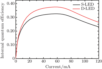
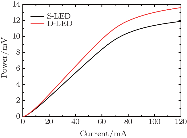
3. Results and discussionIn order to demonstrate the outstanding properties of doubled EBL deep UV-LED, we investigate the light output powers and the internal quantum efficiencies of both structures mentioned above. The output powers each as a function of the current for S-LED and D-LED are plotted in Fig. 2. It can be seen clearly that the difference in output power between these two LEDs is almost negligible when the injection current is below 10 mA. Nevertheless, the output power of D-LED will increase faster than that of S-LED with the injection current increasing when the injection current exceeds 10 mA. Apparently, the output power of D-LED is 13.6 mW, 14.3% higher than that of S-LED, which is 12.9 mV, under the injection current of 120 mA, which indicates the D-LED has more excellent optical performance than the S-LED. Besides, the D-LED also shows a remarkable enhancement of the IQE when the injection current exceeds 10 mA, which means that the IQE of the D-LED is higher than that of the S-LED and more carriers are consumed in the active region. Specifically, the IQE of the D-LED is 37.5% at 60 mA, which is increased by 15.3% as compared with that of the S-LED, which is about 32.6%. These results are shown in Fig. 3.
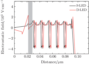
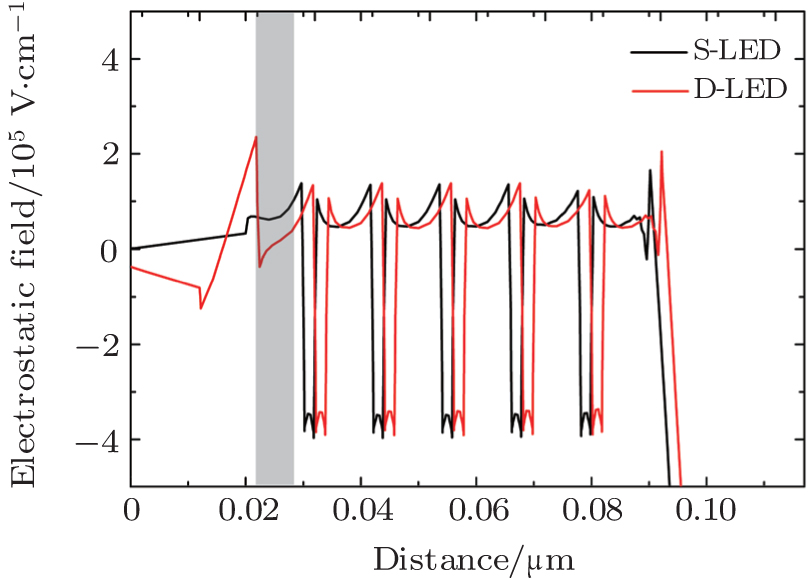
In order to shed light on the origin of the enhancement of the optical performance in detail, the contrastive electrostatic fields and calculated energy band diagrams of both S-LED and D-LED within the active region at 120 mA are shown in Figs. 4 and 5, respectively. Note that the horizontal position of the LED layer is shifted slightly for better observation and a similar manipulation is applied to Fig. 5, and in other diagrams in this test zero reference point is used if need be.
As we can see evidently in Fig. 4, the electrostatic field within the QWs of the D-LED is weaker than that of the S-LED, which leads to the bended band. Therefore, we see the reduced downward bending in the energy band of the QWs in the D-LED, which is beneficial to not only enlarging the spatial overlap of electron and hole wave functions, but also enhancing the hole injection efficiency and suppressing the electron leakage, which coincides with the result of Ref. [35]. What is considered in Ref. [35] is that the strong polarization-induced electrostatic field in the n-EBL reduces the thermal velocity and the mean free path of the hot electrons correspondingly, which can be confirmed by the energy band diagrams.
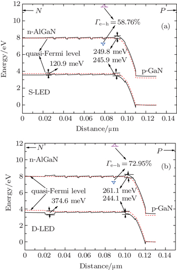
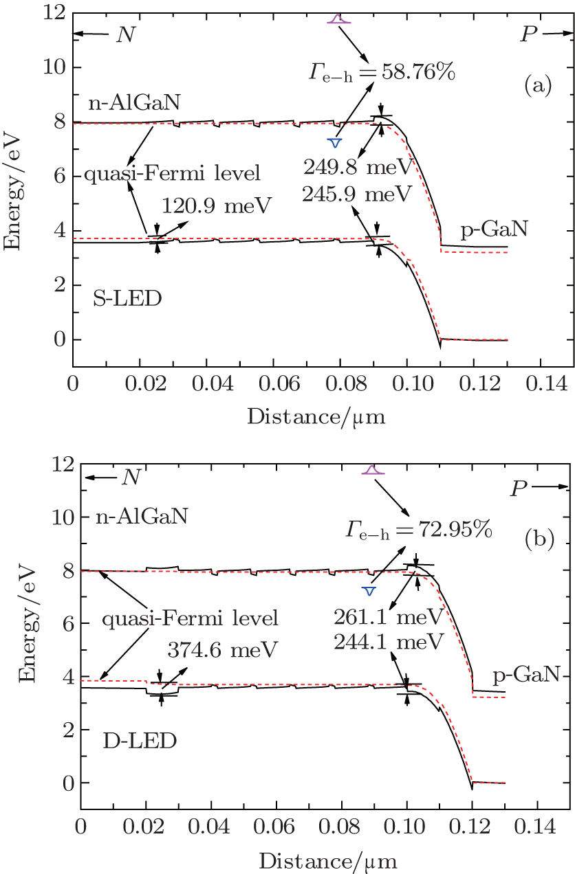
Figures 5(a) and 5(b) show the energy band diagrams in which the electron and hole wave functions (Γe–h) of the S-LED and D-LED overlap at an injection current of 120 mA, respectively.
According to Fig. 5(b), the D-LED with double EBL possesses a higher effective potential barrier height (261.1 meV) for electron, while the S-LED with single EBL has 249.8 meV as shown in Fig. 5(a), which demonstrates that the electron blocking effect in D-LED is better than in S-LED, and electrons have more opportunities to be consumed with holes. The effective potential height for the hole of the D-LED with double EBL (244.1 meV) between the valance band near p-EBL and the last barrier is smaller than that of the S-LED with single EBL at the same part (245.9 meV), therefore the holes can easily be injected into the active region. At the same time, the slighter electrostatic field is also found at the interface between n-EBL and the first barrier in the D-LED as compared with in the S-LED, which is shown in the gray part in Fig. 4. As a result, the curvature of the energy band diagram on the n-side of the D-LED is weaker than that of the S-LED. Therefore, the enhanced hole blocking efficiency appears in the D-LED. We can also find evidences in Fig. 5. It is apparent that the effective potential height for the hole leakage is 374.6 meV in the D-LED near the first barrier and n-side, while the value of the S-LED is only 120.9 meV at the same position, significantly smaller than that of the D-LED. In a word, more holes are confined in the active region for the D-LED.
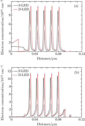
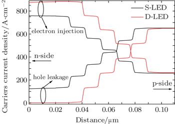
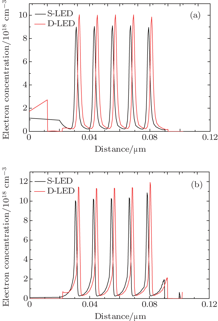
Therefore, the carrier concentrations are certain to be enhanced in the active region for the D-LED. Figure 6 shows the simulated electron and hole distributions near the active regions of the two LEDs at 120 mA. It is apparent that the electron and hole concentrations in the active region of the D-LED are both higher than those of the S-LED, and this will be explained by the following reasons. On the one hand, the induced band bending caused by the mitigatory electrostatic field increases the overlap between the electron and hole wave functions as shown in Fig. 5, the overlaps between the electron and hole wave functions are 58.76% and 72.95% for the S-LED and D-LED, respectively, the increase of the overlap between electron and hole wave functions results in the contribution of more carriers to radioactive recombination, and thus more carriers are consumed in QWs. On the other hand, the hole injection efficiency and electron blocking effect in the p-side are improved because of the optimized effective barrier height. In addition, the added n-AlGaN can not only suppress the hole overflow to the n-side region, but also acts as an electron emitting source, then more electrons will inject into the active region. In order to demonstrate that more holes are consumed in QWs and more electrons are injected into QWs more visibly, we explore the carrier current densities of the two structures at 120 mA, which are shown in Fig. 7.
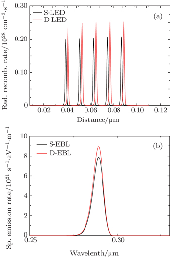
The hole leakage for the S-LED is 129.2 A/cm2, while the hole leakage for the D-LED is almost zero. The electron injection in the first QW for the D-LED is 883.8 A/cm2, vastly larger than that for the S-LED, which is 757.1 A/cm2. Obviously, the radioactive recombination rate and spontaneous emission rate, plotted in Fig. 8, of the D-LED are significantly higher than those of the S-LED at 120 mA, which is attributed to the improved overlap between electron and hole wave functions analyzed above and higher carrier concentrations in the active region presented in Fig. 6. Figure 8(a) shows that the radioactive recombination rates in the active region of the D-LED are improved markedly in comparison with those of the S-LED, which in turn accelerates the rise of the spontaneous emission rates as shown in Fig. 8(b).
4. ConclusionsIn this paper, the AlGaN-based DUV-LEDs with double EBLs inside the active region are investigated theoretically by using APSYS software. The simulation suggests that when both p-EBL and n-EBL are adopted, the polarization-induced electrostatic field within the QWs is mitigated, so does the electrostatic field between the n-side and the active region. As a result, the overlap between electron and hole wave functions is improved compared with the scenario of a conventional LED with a single p-EBL, the efficiency of the hole injected into the active region is increased and the carrier blocking effect is enhanced. Finally, the optical performances of the AlGaN LED with both the p-EBL and n-EBL at high current are optimized, and the larger recombination rate, a much higher light output power and IQE are obtained. We can expect that the double EBLs plays an important role in improving the performances of AlGaN-based DUV-LED. So, the technological process and grown conditions of this method are simpler than those of other complicated EBLs.


 , Li Xu-Na, Sun Hao, Fan Xuan-Cong, Zhang Zhu-Ding, Guo Zhi-You]