Current-induced nonequilibrium spin polarization in semiconductor-nanowire/s-wave superconductor junctions with strong spin–orbit coupling
Liu Nai-Qing, Huang Li-Jie, Wang Rui-Qiang, Hu Liang-Bin†,
Guangdong Provincial Key Laboratory of Quantum Engineering and Quantum Materials, School of Physics and Telecommunication Engineering, South China Normal University, Guangzhou 510631, China


† Corresponding author. E-mail: lbhu26@yahoo.com

Project supported by the National Natural Science Foundation of China (Grant No. 11474106).

Abstract
Abstract

We have studied the characteristics of current-induced nonequilibrium spin polarization in semiconductor-nanowire/s-wave superconductor junctions with strong spin–orbit coupling. It was found that within some parameter regions the magnitude of the current-induced nonequilibrium spin polarization density in such structures will increase (or decrease) with the decrease (or increase) of the charge current density, in contrast to that found in normal spin–orbit coupled semiconductor structures. It was also found that the unusual characteristics of the current-induced nonequilibrium spin polarization in such structures can be well explained by the effect of the Andreev reflection.

1. Introduction

Semiconductor spintronics has been an active research field in recent years because of its potential applications in electronic devices and quantum computation.[16] An important research subject in semiconductor spintronics is how to generate nonequilibrium spin polarization or spin current in nonmagnetic semiconductor structures by purely electrical means.[1,3,6] This is a prerequisite for integrating spin effects into standard lithographic semiconductor structures. It was theoretically predicted and experimentally verified that, in the presence of strong spin–orbit coupling, nonequilibrium spin polarization or spin current can be generated in nonmagnetic semiconductor structures by purely electrical means. The most prominent examples are the discoveries of the phenomena of spin Hall effect (SHE)[710] and current-induced spin polarization (CISP),[11,12] both of which have been intensively studied in recent years.[1324] Both these phenomena rely on spin–orbit interaction of charge carriers,[5] but the mechanisms leading to them are different. In the phenomenon of SHE, a longitudinal charge current induces a transverse spin current and hence leads to nonequilibrium spin accumulation at the edges of the sample. In the phenomenon of CISP, nonequilibrium spin polarization is induced by momentum-dependent effective magnetic field due to spin–orbit coupling and its mechanism does not involve the very concept of spin current,[25] i.e., nonequilibrium spin polarization can be generated by the flow of a pure charge current, without bulk spin current.[6]

In previous studies about the phenomenon of CISP, only normal spin–orbit coupled semiconductor structures have been considered. An interesting question is that what characteristics it will have if a spin–orbit coupled semiconductor is in contact with a superconductor. It is well known that in low-dimensional semiconductor/superconductor hybrid structures, spin–orbit coupling may affect significantly electronic transport properties of the structures,[2631] as in the case of exchange field in ferromagnet/superconductor hybrid structures.[32,33] For example, it was shown in Ref. [27] that specular Andreev reflection can occur in a hybrid system of a two-dimensional electron gas with Rashba spin–orbit coupling and a d-wave superconductor, as predicted in the graphene-based normal-metal/superconductor junction.[34,35] In Ref. [28] an interesting quantum plateau behavior was predicted for the Andreev reflection in one-dimensional semiconductor quantum wire/s-wave superconductor junctions with strong spin–orbit coupling. These studies suggest that the interplay of strong spin–orbit coupling and superconducting proximity effect may lead to some interesting transport properties in low-dimensional semiconductor/superconductor hybrid structures. But to the best of our knowledge, what influence the superconducting proximity effect might have on current-induced nonequilibrium spin polarization in spin–orbit coupled nonmagnetic semiconductor structures is still not very clear. To explore possible consequences of the superconducting proximity effect on current-induced nonequilibrium spin polarization in such structures, in this paper we present a detailed theoretical investigation on the characteristics of current-induced nonequilibrium spin polarization in semiconductor-nanowire/s-wave superconductor junctions with strong spin–orbit coupling. It is found that current-induced nonequilibrium spin polarization in such structures may exhibit some unusual characteristics, in contrast to that found in normal spin–orbit coupled semiconductor structures. It is also found that such unusual characteristics can be well explained by the consequences of the Andreev reflection due to the superconducting proximity effect. Such unusual characteristics may be useful for the practical applications of such hybrid structures.

The paper is organized as follows. In Section 2 we provide some details of the model considered and the formulation for the calculation of charge current and current-induced nonequilibrium spin polarization. In Section 3 we present some numerical results obtained by the formulation. The physical implications of the results will be discussed in some detail. Finally, a brief summary is given in the end of the paper.

2. Model and formulation

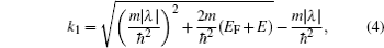
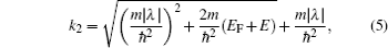
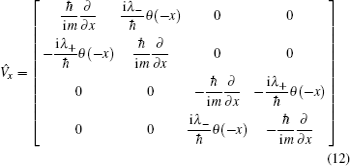
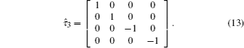
We consider a ballistic one-dimensional semiconductor-nanowire/s-wave superconductor junction along the x direction. We assume that spin–orbit coupling presents only in the semiconductor (SM) region. The spin–orbit coupling may arise either from structural or inversion asymmetry of the semiconductor, which are termed Rashba or Dresselhaus spin–orbit coupling in the literature.[3639] We denote the strength of Rashba spin–orbit coupling as αR and the strength of Dresselhaus spin–orbit coupling as βD. The energy gap in the superconductor (S) region is denoted as Δ. The interface of the SM and S regions is located at x = 0 and the interfacial barrier potential is described by the delta function U(x) = U0δ (x). We use the following convention for Nambu spinors: Ψ(x) = (u(x),u(x),v(x),v(x))T, in which u(↓) and v(↓) denotes wave functions of electrons and holes with up (down) spin, respectively. Then the effective Hamiltonian for the entire structure can be written as

where λ± = αR ± iβD, θ (x) is the step function, ξk = ħ2k2/2mEF, with the Fermi energy EF. For simplicity, we neglect the difference of the effective mass in the SM and S regions. The effective mass in SM is usually smaller than that in S. This effect is equivalent to the increase of the interface barrier.

The wave function in the SM and S regions can be represented using eigenfunctions of the Hamiltonian (1). In the SM region (x < 0), due to the presence of spin–orbit coupling, for a given eigenenergy E, there are two degenerated electron (or hole) states. On the other hand, due to the superconducting proximity effect, an electron incident on the interface of the two regions can be reflected either as an electron (normal reflection) or as a hole (Andreev reflection[40]). Thus, the general form of the wave function on the SM side can be expressed either as

or as

where Ψ1 and Ψ2 describe two degenerated electronic states with the same incident energy E, a1(2) and b1(2) denote Andreev reflection coefficients and c1(2) and d1(2) normal reflection coefficients, respectively. The wave numbers k1, k2, and are all functions of the energy E and are given, respectively, by

Similarly, in the S region (x > 0), the wave function can be expressed as

where e1(2), f1(2), g1(2), and h1(2) are transmission coefficients, ke and kh denote the wave numbers of electron-like and hole-like quasi-particles with the same quasiparticle energy E, with

and

and u0 and v0 are defined by

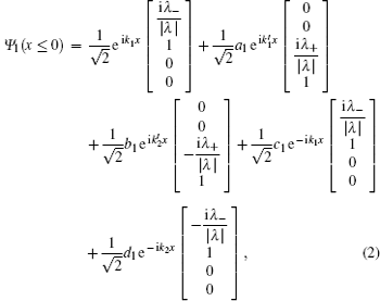
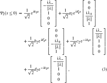
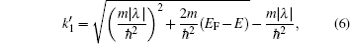
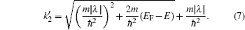
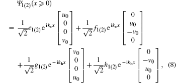
There are eight coefficients in the expressions of the wave functions Ψ1(2), which need to be determined self-consistently through the following boundary condition:

where x = ħ−1∂H/∂kx is the velocity operator,

and is defined by

From the boundary conditions (10) and (11), the eight coefficients in the expressions of the wave functions Ψ1(2) can be determined self-consistently for a given energy E.

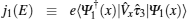
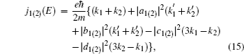
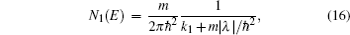
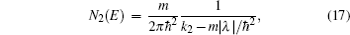
When a bias voltage V is applied, the charge current and the current-induced nonequilibrium spin polarization can be calculated using the wave functions obtained above. The procedure is as following. First, we calculate the expectation values of charge current and current-induced spin polarization for the complete sets of the eigenfunctions. Next we sum the expectation values multiplied by the corresponding distribution functions. Then the charge current density can be expressed as

Here and , which can be expressed explicitly as

and N1(E) and N2(E) are density of states of the two spin–orbit split bands of the semiconductor nanowire, with

where k1 and k2 are given by Eqs. (4) and (5). In Eq. (15), the first term represents the current contribution from the incident waves, the second and the third terms (i.e., the terms proportional to |a1(2)|2 and |b1(2)|2) are the current contribution from the Andreev reflection, and the last two terms (i.e., the terms proportional to |c1(2)|2 and |d1(2)|2) are the current reduction due to the normal reflection. In the absence of spin–orbit coupling, equation (14) will reduce to the standard BTK current formula.[40]

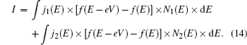
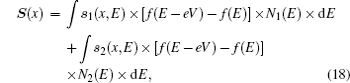
The density of the current-induced nonequilibrium spin polarization is position-dependent and can be calculated similarly as the charge current, and the result can be can expressed as

where S(x) denotes the density of the current-induced nonequilibrium spin polarization at position x, and and , with the Pauli matrices σ operating in spin space and τz operating in particle–hole space, respectively.

3. Results and discussions

In this section we present some numerical results obtained by the formulation introduced above. For convenience, we define the strength of Rashba and Dresselhaus spin–orbit coupling by two dimensionless parameters α and β: α ≡ 2R/ħ2kF and β ≡ 2D/ħ2kF, with the Fermi wave number kF. The height of the interface barrier is defined by a dimensionless parameter Z ≡ 2mU0/ħ2kF. The superconducting gap Δ will be measured by the Fermi energy EF. The spin polarization density will be measured in unit of ħ/lF, with the Fermi wavelength lF. We confine our discussions to zero temperature.

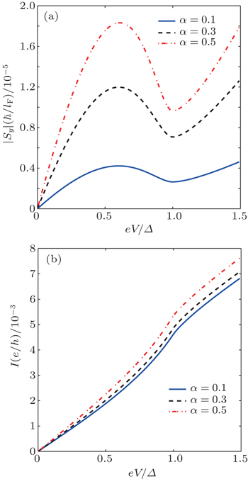
First we study the variation of the magnitude of the current-induced spin polarization density in SM with the increase of the bias voltage. The magnitude of the current-induced spin polarization density in SM is position-dependent and we take a sample point (defined by |kFx| = 50) as the example. In Fig. 1(a) we show the variation of the magnitude of the current-induced spin polarization density at the sample point in SM with the increase of the bias voltage for several different spin–orbit coupling strengths. For comparison, in Fig. 1(b) we show the corresponding variation of the charge current density. From Fig. 1(a) one can see that, in the voltage region where eV is smaller than the superconducting gap, the magnitude of the current-induced spin polarization density will increase first with the increase of the bias voltage and then turn to decrease with the further increase of the bias voltage. As eV is increased further and exceeds the superconducting gap, the magnitude of the current-induced spin polarization density will turn again to increase with the increase of the bias voltage. In contrast to the current-induced spin polarization, the magnitude of the charge current density increases monotonically with the increase of the bias voltage, as shown in Fig. 1(b).

Fig. 1. (a) The variation of the magnitude of the current-induced spin polarization density at a sample point (defined by |kFx| = 50) in SM with the increase of the bias voltage. (b) The corresponding variation of the charge current density with the increase of the bias voltage. The parameters are: Δ/EF = 0.001, Z = 1, β =0, and α is shown in the inset of the figures. For the cases of β =0, the direction of the current-induced spin polarization is parallel to the y axis. If both α and β are not zero, both x and y components of the spin polarization will be non-vanishing. In such cases the variation of the spin polarization density with the increase of the bias voltage is still similar to that as shown in Fig.
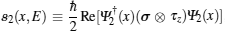
 1(a) and hence not shown explicitly.

From Fig. 1(a) and Fig. 1(b), one can see that there is a voltage region within which the magnitude of the current-induced spin polarization density decreases with the increase of the charge current density. This characteristic is unusual and can be explained theoretically by the consequences of the Andreev reflection (AR) due to the superconducting proximity effect. To explain this point more clearly, let us iterate briefly the mechanism of CISP in normal spin–orbit coupled systems. From the theoretical point of view, the spin–orbit coupling of charge carriers can act as a momentum-dependent effective magnetic field. If this effective magnetic field is sufficiently strong, the direction of an electron's spin will tend to align with it. But in the absence of charge current flow, this effective magnetic field does not lead to a net spin polarization. This is due to the fact that, in the equilibrium state, the number of electrons occupying the state with wave vector k is always equal to that occupying the state with opposite wave vector −k, and when the wave vector of an electron is changed from k to −k, the direction of the effective magnetic field due to spin–orbit coupling is also reversed. This symmetry will be broken in the presence of charge current flow. When a charge current flows through the system, the number of electrons moving in the direction of the charge current is different from that moving in the opposite direction, and due to this imbalance, the momentum-dependent effective magnetic field due to spin–orbit coupling can lead to a net spin polarization. According to this physical picture of CISP, the magnitude of the current-induced spin polarization density will increase with the increase of the charge current density. This is the usual case found in normal spin–orbit coupled semiconductor structures. However, in a semiconductor/superconductor junction with spin–orbit coupling, in addition to the mechanism mentioned above, the process of the Andreev reflection due to the superconducting proximity effect can also affect substantially the magnitude of the current-induced spin polarization. In the process of the Andreev reflection, a pair of electrons with opposite spins are transmitted to the S region as a Cooper pair. This process can enhance the tunneling current, but since a Cooper pair has two opposite spins, it will suppress the magnitude of the current-induced spin polarization. So within the parameter regions where the AR process is significant, the magnitude of the current-induced spin polarization may be suppressed by the increase of the AR effect. To illustrate this point more clearly, in Figs. 2(a) and 2(b) we plot the AR probabilities A1 (≡ |a1|2) and B2 (≡ |b2|2) as a function of eV/Δ. (For the cases shown in Fig. 1, the dominant AR processes are described by the terms proportional to a1 and b2 in the wave functions Ψ1 and Ψ2, respectively.) By comparing Fig. 1 and Fig. 2, one can see clearly that the voltage region within which the magnitude of the current-induced spin polarization density decreases with the increase of the charge current density coincides with the voltage region within which the AR probabilities A1 and B2 increase substantially.

Fig. 2. (a) The variation of the Andreev reflection probability A1 with the increase of the bias voltage. (b) The variation of the Andreev reflection probability B2 with the increase of the bias voltage. The parameters used are the same as in Fig. 1. The energy of incident electrons is set at the Fermi level.

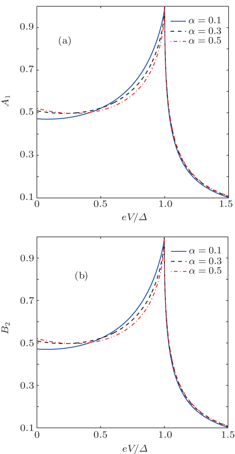
To show more clearly the unusual characteristics of CISP in the structures considered, in Figs. 3(a) and 3(b) we also plot the derivatives of the magnitude of the current-induced spin polarization density and the charge current density with respect to the bias voltage as a function of eV/Δ. From Figs. 3(a) and 3(b) one can see that the variation of d|S|/dV with the increase of the bias voltage is also significantly different from that of dI/dV. The significant difference between them can also be accounted for by the consequences of the Andreev reflection.

Fig. 3. (a) The derivative d|S|/dV, a sample point in SM as a function of the bias voltage. (b) The derivative dI/dV (i.e., the differential conductance) as a function of the bias voltage. The parameters are the same as used in Fig. 1.

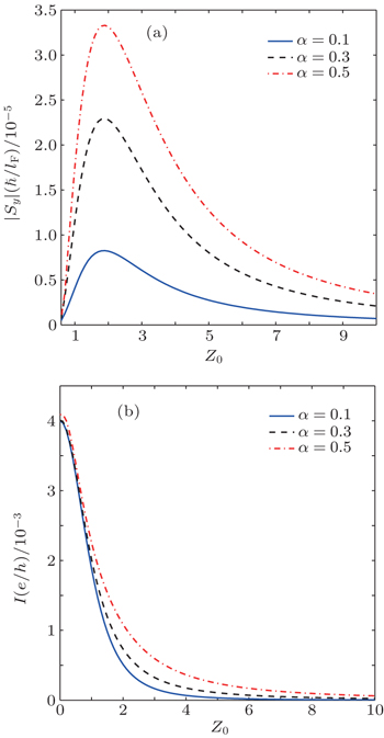
Next, we study the effect of the interface barrier height on the magnitude of the current-induced spin polarization density. In Fig. 4(a) we show the variation of the magnitude of the current-induced spin polarization density at a sample point in SM with the increase of the interface barrier height (characterized by the dimensionless parameter Z) for several different spin–orbit coupling strengths. For comparison, in Fig. 4(b) we show the corresponding variation of the charge current density. From Figs. 4(a) and 4(b) one can see that, while the magnitude of the charge current density decreases rapidly and monotonically with the increase of the interface barrier height, the magnitude of the current-induced spin polarization density is first enhanced as the interface barrier increases from zero. This unusual relation between charge current and current-induced spin polarization can also be accounted for by the consequences of the Andreev reflection. As the interface barrier height increases from zero, both the Andreev reflection and the normal transmission will be decreased. The decrease of both the Andreev reflection and the normal transmission will reduce the magnitude of the charge current density, so the magnitude of the charge current density decreases rapidly and monotonically with the increase of the interface barrier height. But for the current-induced nonequilibrium spin polarization, the decrease of the Andreev reflection can enhance its magnitude, while the decrease of the normal transmission will reduce its magnitude. Due to the combined effect of these two opposite factors, unlike the magnitude of the charge current density, the magnitude of the current-induced spin polarization density can be enhanced by the decrease of the Andreev reflection as the interface barrier height increases from zero, providing that the enhancement effect due to the decrease of the Andreev reflection is more significant than the reduction effect due to the decrease of the normal transmission. As the barrier height is increased further, the reduction effect due to the decrease of the normal transmission will become more significant than the enhancement effect due to the decrease of the Andreev reflection, and then the magnitude of the current-induced spin polarization density also turns to decrease rapidly and monotonically with the increase of the barrier height, like the charge current. To illustrate this point more clearly, in Figs. 5(a) and 5(b) we plot the AR probabilities A1 (≡ |a1|2) and B2 (≡ |b2|2) as a function of the parameter Z, from which one can see that the parameter region within which the magnitude of the current-induced spin polarization density increases with the decrease of the charge current density coincides with the parameter region within which the AR probabilities decrease substantially.

Fig. 4. (a) The variation of the magnitude of the current-induced spin polarization density at a sample point (defined by |kFx|=50) in SM with the increase of the interface barrier height (characterized by the dimensionless parameter Z) for several different spin–orbit coupling strengths. (b) The corresponding variation of the charge current density with the increase of the interface barrier height. The parameters are: Δ/EF = 0.001, eV/Δ = 0.5, β = 0, and α is shown in the inset of the figures.
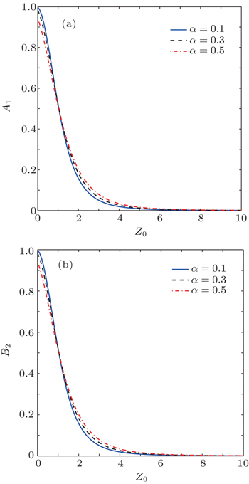
Fig. 5. (a) The variation of the Andreev reflection probability A1 with the increase of the interface barrier height. (b) The variation of the Andreev reflection probability B2 with the increase of the interface barrier height. The parameters used are the same as in Fig. 4. The energy of incident electrons is set at the Fermi level.
4. Summary

In summary, we have studied the characteristics of current-induced nonequilibrium spin polarization in semiconductor–nanowire/s-wave superconductor junctions with strong spin–orbit coupling. It was found that, due to the consequences of the Andreev reflection induced by the superconducting proximity effect, there are some parameter regions within which the magnitude of the current-induced nonequilibrium spin polarization density will increase (or decrease) with the decrease (or increase) of the charge current density, in contrast to that found in normal spin–orbit coupled semiconductor structures. These unusual characteristics can be taken as a clear indication of the suppression or enhancement of the Andreev reflection in such structures. The results obtained may be useful for a better understanding of the unusual properties of low-dimensional semiconductor/superconductor hybrid structures with strong spin–orbit coupling.

Reference
1Zutic IFabian JDas Sarma S 2004 Rev. Mod. Phys. 76 323
2Awschalom D DLoss DSamarth N2002Semiconductor Spintronics and Quantum ComputationBerlinSpringer
3Awschalom D DFlatte M E 2007 Nat. Phys. 3 153
4Wu M WJiang J HWeng M Q 2010 Phys. Rep. 493 61
5Winkler R2003Spin-Orbit Coupling Effects in Two Dimensional Electron and Hole SystemsBerlinSpringer
6Yang C LWang J LGe W KCui L JZhang Y P2007Physics367(in Chinese)
7Murakami SNaogaosa NZhang S C 2003 Science 301 1348
8Sinova JCulcer DNiu QSinitsyn N AJungwirth TMacDonald A H 2004 Phys. Rev. Lett. 92 126603
9Kato Y KMyers R CGossard A CAwschalom D D 2004 Science 306 1910
10Wunderlich JKastner BSinova JJungwirth T 2005 Phys. Rev. Lett. 94 047204
11Edelstein V M 1990 Solid State Commun. 73 233
12Kato Y KMyers R CGossard A CAwschalom D D 2005 Appl. Phys. Lett. 87 022503
13Zyuzin V ASilvestrov P GMishchenko E G 2007 Phys. Rev. Lett. 99 106601
14Bokes PCorsetti FGodby R W 2008 Phys. Rev. Lett. 101 046402
15Silvestrov P GZyuzin V AMishchenko E G 2009 Phys. Rev. Lett. 102 196802
16Rech JMicklitz TMatveev K A 2009 Phys. Rev. Lett. 102 116402
17Teodorescu VWinkler R 2009 Phys. Rev. B 80 041311
18Bokes PHorvath F 2010 Phys. Rev. B 81 125302
19Sonin E B 2010 Phys. Rev. B 81 113304
20Duckheim MLoss DScheid MRichter KAdagideli IJacquod P 2010 Phys. Rev. B 81 085303
21Linder JYokoyama TSudbo A 2010 Phys. Rev. B 81 075312
22Koralek J DWeber C POrenstein JBernevig B AZhang S CMack SAwschalom D D 2009 Nature 458 610
23Walser M PReichl CWegscheider WSalis G 2012 Nat. Phys. 8 757
24Kunihashi YKohda MNitta J 2012 Phys. Rev. B 85 035321
25Shi J RZhang PXiao DNiu Q2006Physics35720(in Chinese)
26Linder JYokoyama T 2011 Phys. Rev. Lett. 106 237201
27Lv BZhang CMa Z S 2012 Phys. Rev. Lett. 108 077002
28Xu L TLi X Q 2014 Europhys. Lett. 108 67013
29Hao X JLi H OTu TZhou CCao GGuo G CGuo G PFung W YJi Z QLu W 2011 Phys. Rev. B 84 195448
30Takei SGalitski V 2012 Phys. Rev. B 86 054521
31Bergeret F STokatly I V 2014 Phys. Rev. B 89 134517
32de Jong M J MBeenakker C W J 1995 Phys. Rev. Lett. 74 1657
33Zutic IWalls O T 2000 Phys. Rev. B 61 1555
34Beenakker C W J 2006 Phys. Rev. Lett. 97 067007
35Beenakker C W J 2008 Rev. Mod. Phys. 80 1337
36Bychkov YRashba E I 1984 J. Phys. C 17 6039
37Dresselhaus G 1955 Phys. Rev. 100 580
38Yang JZhang XMiao R D 2014 Acta Phys. Sin. 63 217202 (in Chinese)
39Tang H ZZhai L XShen MLiu J J 2015 Chin. Phys. B 24 030303
40Blonder G ETinkham MKlapwijk T M 1982 Phys. Rev. B 25 4515