


Detection and formation mechanism of micro-defects in ultrafine pitch Cu—Cu direct bonding
[Liu Zi-Yu 1 , Cai Jian 1, 2, †,  , Wang Qian 1 , Chen Yu 1 ]
, Wang Qian 1 , Chen Yu 1 ]
|
|


† Corresponding author. E-mail:
Project supported by the National Natural Science Foundation of China (Grant No. 61274111) and the National Basic Research Program of China (Grant No. 2015CB057205).
In this paper, Cu–Cu interconnects with ultrafine pad pitches of 6 μm, 8 μm, and 15 μm are implemented on the 12 inch wafers by a direct bonding process. Defects are not found by traditional non-destructive (NDT) c-mode scanning acoustic microscopy (c-SAM). However, cross sectional observation of bonding interfaces reveals that micro-defects such as micro seams are located at SiO 2 bonding interfaces. In order to examine the micro-defects in the ultra-fine pitch direct bonding process by the NDT technology, a novel “defect-enlarged approach” is proposed. The bonded dies are first annealed in an N 2 oven at 300 °C for a few hours and then cooled quickly in air. The c-SAM scanning images show large defects at the place where nothing can be detected by c-SAM before this treatment. Cross sectional observation of the bonding interfaces indicates that these defects consist of large size micro seams at the SiO 2 bonding interface, especially near Cu pads with an ultrafine pitch of 6 μm. However, these large defects disappear after several hours at room temperature, observed by c-SAM. It is inferred that the disappearance of these defects inspected by the “defect-enlarged approach” results from the combination of intrinsic micro seams and “weak” bonds in the silicon oxide layer. Then the underlying physical mechanism of these micro-defects is proposed, which is influenced by Cu pad surface topology and bonding models.
Cu–Cu bonding is an attractive choice for three-dimensional (3D) integration because it can achieve ultrafine pitch, low cost, high electrical conductivity, thermal conductivity, and electromigration reliability. [ 1 – 4 ] Traditional thermo-compression technology needs a bonding temperature higher than 300 °C and a bonding pressure of more than 200 kPa. [ 3 , 5 , 6 ] The high bonding temperature is a challenge, for aspects such as misalignment, thermal stress and process reliability. [ 7 ] Furthermore, the high bonding pressure will introduce cracks into ultra-thin chip interconnection. In the direct bonding process, silicon oxide is pre-bonded by the hydrogen bond then the nearby Cu–Cu interfaces tightly contact each other due to the stress obtained from silicon oxide. [ 8 – 10 ] So neither extra bonding temperature nor pressure is exerted on the silicon wafer in the pre-bonding process. Therefore, Cu–Cu direct bonding technology is considered as one of the most promising processes used for 3D integration, and many studies of the process optimization [ 8 , 10 , 11 ] have been conducted. As the integration density increases, the bonding pitch needs to be reduced sharply and simultaneously micro-defects such as voids and seams may increase in the direct bonding process. Besides, the bonding interfaces are complicated including SiO 2 –SiO 2 , Cu–Cu, and SiO 2 –Cu. [ 8 ] Usually the SiO 2 –SiO 2 interfaces contain a bonded area, a “weak” bonded area and an un-bonded area. [ 12 ] The bonded area is defined as the area bonded with a covalent bond and the “weak” bonded area is treated as the interface with a mediate state between bonded and un-bonded. However, few studies have been performed on the detection of “weak” bonds and micro-defects of several micrometers in size especially by nondestructive testing (NDT) technologies. Defect detection in an electronic device is attracting more and more attention these days due to its practical and scientific significance. [ 13 , 14 ] Though a traditional c-mode scanning acoustic microscope (c-SAM) has been used to detect the defects at the wafer level, [ 1 , 8 , 15 ] there have been no data available about the micro-defects or “weak” bonds detected by NDT technologies to date because the resolution of c-SAM is limited by material and distance. Additionally “weak” bonds such as the hydrogen bond cannot be inspected by c-SAM nor other NDTs. These types of micro-defects and “weak” bonds may not be found from the cross sectional observation nor from the initial electrical tests, but they may cause long-term device reliability.
In this work, a novel approach is proposed to inspect the micro-defects with several micrometers in size after the ultrafine pitch Cu–Cu direct bonding has been implemented. Firstly, Cu–Cu interconnects with ultra-fine pitches of 6 μm, 8 μm and 15 μm are fabricated by the direct bonding process on the 12 inch wafers with a thickness of 750 μm. Defects at the bonding interfaces are not found by traditional c-SAM observation. In order to detect micro-detects such as micro seams and “weak” bonds, a “defect-enlarged approach” is applied, in which the bonded dies are annealed at 300 °C for a few hours and then cooled quickly in air. The cSAM observation is subsequently carried out and the enlarged micro-detects are detected. However, enlarged micro-detects recover or disappear in the c-SAM images after several hours. Based on these observations, the defect type and formation mechanism are inferred and discussed.
The process flow chart of Cu–Cu wafer level direct bonding is illustrated in Fig.
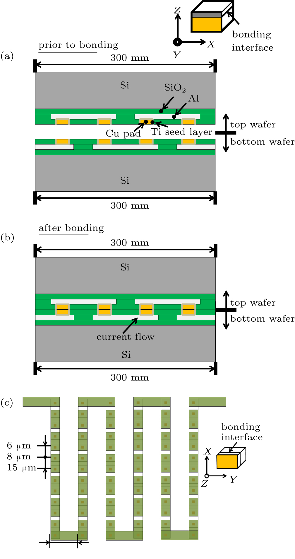 | Fig. 1. Process flow illustration of Cu–Cu direct bonding (a) prior to and (b) after bonding, and (c) bonding structure design. |
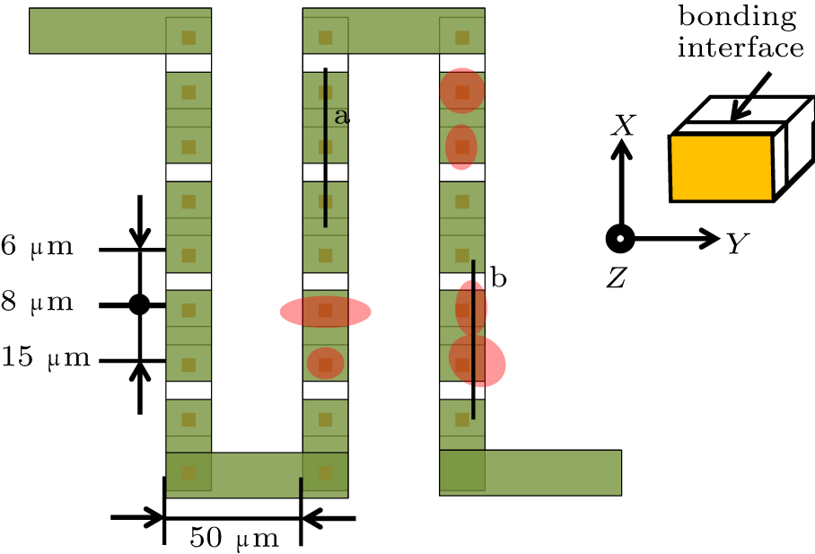
After bonding, bonded wafers were sliced into dies with different sizes, each of which included a daisy chain structure with all the bonding pad pitches. Then c-SAM (KSI SAM 300) was used to examine the defects such as large voids or un-bonded area. However, for the bonding interfaces with no large defects detected by c-SAM, micro seams were found in crosssectional observation by scanning electron microscopy (SEM, TESCAN LYRA3 FEG-SEM) near some Cu bonding pads, especially at the ultrafine pitch of 6 μm. Cross-sectional observation was destructive and partial so it cannot be used to detect all the micro-defects. In order to distinguish the dies with no micro-defects, a novel approach was adopted to explore the micro-defects at the bonding interfaces. It included the annealing process and quick cooling. The bonded die was annealed for a few hours in the N 2 oven and subsequently cooled quickly in air. Then c-SAM detection was used again to find out whether there are enlarged micro-defects. Besides, in order to clarify the formation mechanism of these micro-defects, the bonding interfaces were examined by SEM observation before and after the annealing process.
Though large defects are not detected by traditional c-SAM scanning because of low theoretical resolution of traditional c-SAM, micro seams are found after cross sectional observations of different bonding pitches at some bonding interfaces. Consequently, a modified NDT approach is proposed. Ten samples are dealt with by this approach and enlarged micro-defects are found by c-SAM in three dies. Cross sectional observations are used to characterize the bonding interfaces of the enlarged micro-defects. Furthermore, enlarged micro-defects recover and disappear in the c-SAM images after several hours. Subsequently, the physical mechanism of micro-defects is inferred and discussed.
The c-SAM scanning is adopted to detect large defects such as un-bonded areas at the bonding interfaces. Owing to the high longitudinal sound velocity of silicon (8430 m/s), [ 16 ] the theoretical resolution of c-SAM imaging is relatively low. Though a high frequency ultrasonic probe can be used, the penetration depth is much lower than 750 μm, which limits the application of c-SAM in the thick bonded wafers. In order to obtain enough of a penetration depth, a 150-MHz ultrasonic probe is adopted in the c-SAM scanning process and the theoretical resolution is calculated from the following equation:

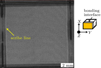
 | Fig. 2. C-SAM detection of large defects for sliced die after direct bonding process. |
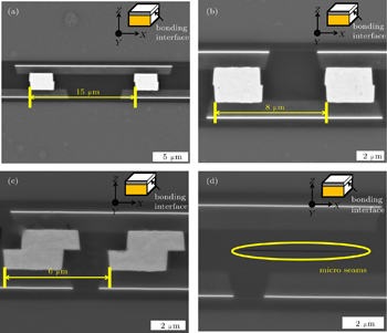
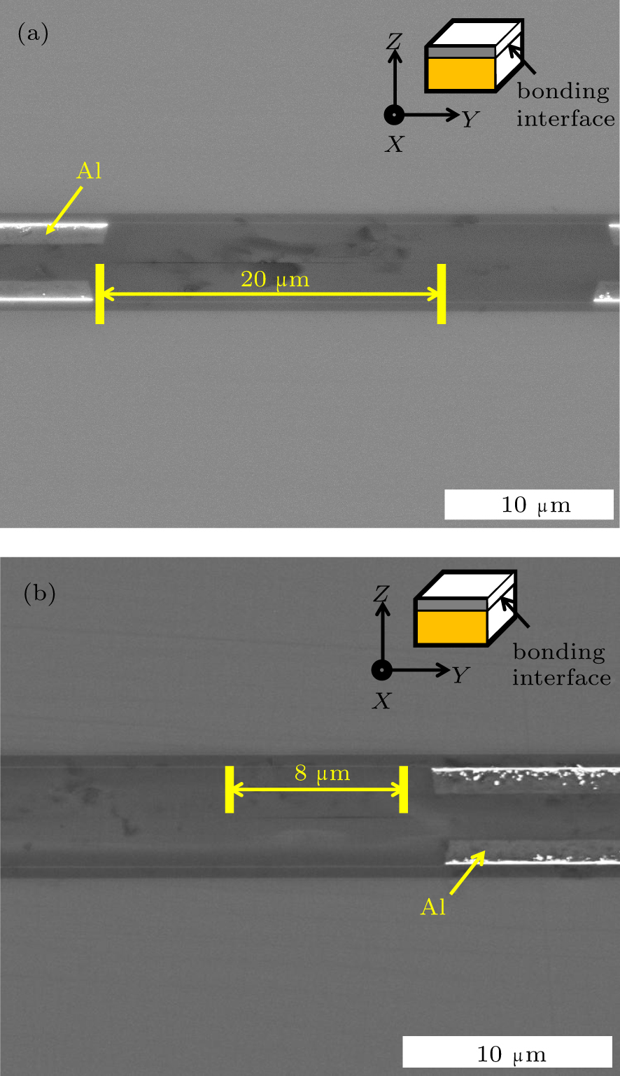
Interface microstructures of different pitches are then observed by SEM, which can be shown in Figs.
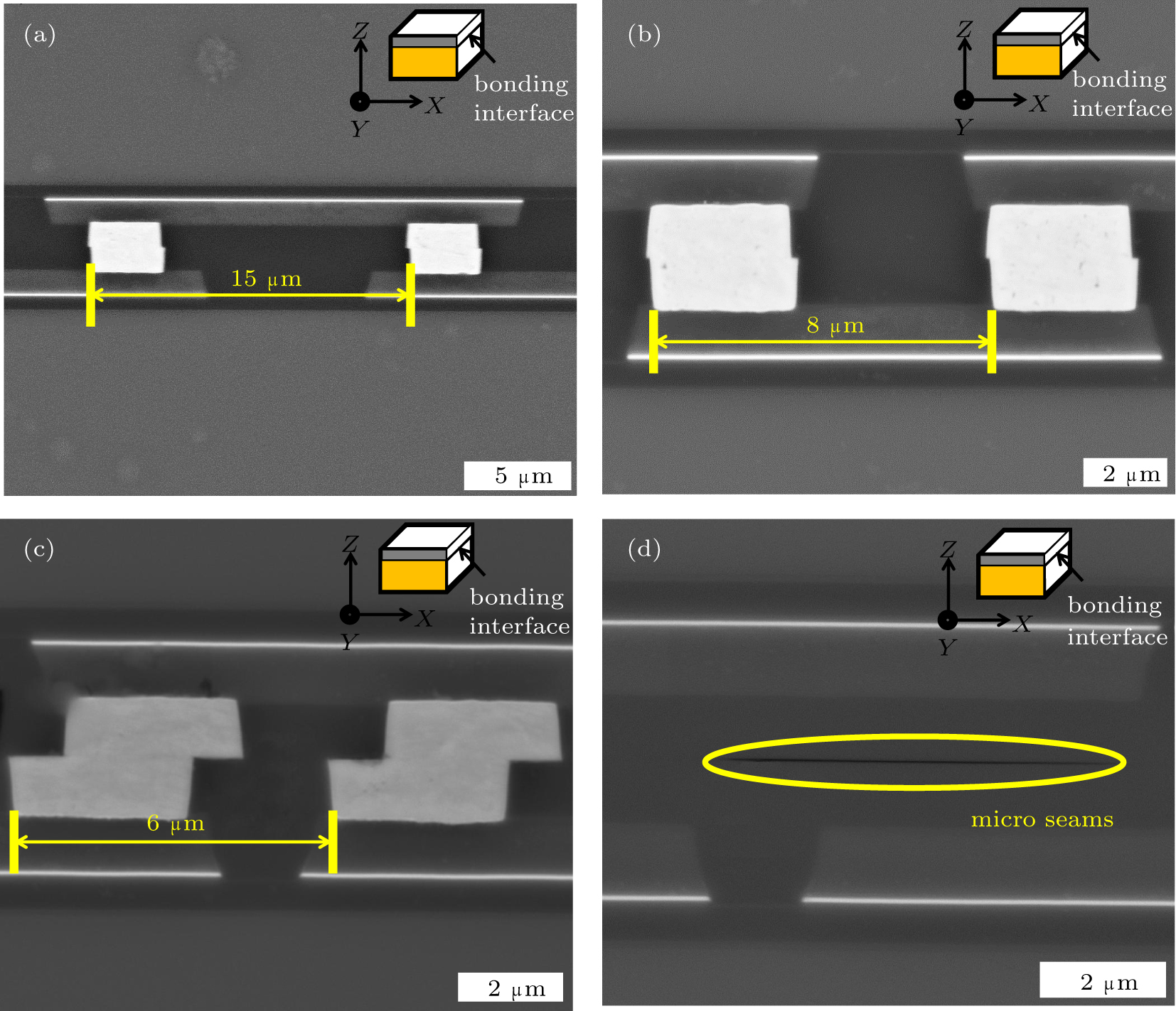 | Fig. 3. Interface morphologies observation by SEM for the pitches of (a) 15 μm, (b) 8 μm, (c) 6 μm, and (d) seams near the bonded Cu pad. |
The approach is composed of a defect-enlarging process and c-SAM scanning, so it is named the “defect-enlarged approach”. First, the tested dies are annealed in an oven with N 2 atmosphere at 300 °C for a few hours. Then they are transferred out of the oven quickly and cooled in air. The c-SAM detection is used to explore micro-defects. In this approach, the annealing process is of benefit to inter-diffusion, so Cu–Cu or SiO 2 –SiO 2 interfaces bonded in the direct bonding process are strengthened. However, the micro-defects such as seams or voids of the SiO 2 bonding interface will not change in the annealing process because the interior of the micro-defect is in a vacuum state. After a quick cooling process, these micro-defects will be enlarged due to thermal expansion.
Ten as-bonded samples are examined by the c-SAM images and no defect is found, which is the same as the scenario in Fig.
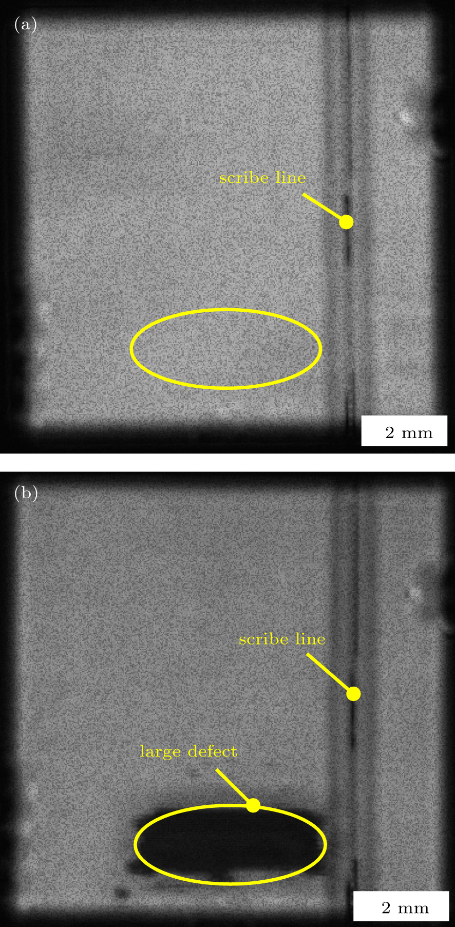 | Fig. 4. The c-SAM images for sliced dies after the direct bonding process: (a) as-bonded, (b) after annealing and quick cooling. |
These large defects detected by the proposed approach might originate from the combination of micro seams and “weak” bonds at the silicon oxide bonding interface. In order to identify the assumption, SEM observation is carried out to examine the interface morphologies of the large defects found by the “defect-enlarged approach”. Figure
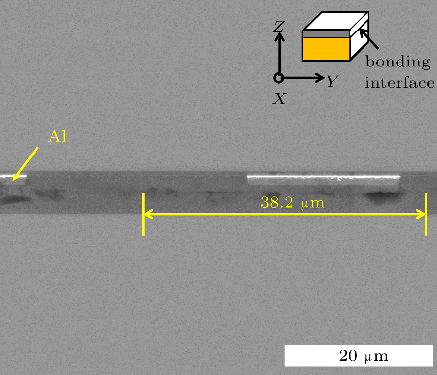 | Fig. 5. SEM image of the interface morphology and microstructure after annealing and quick cooling. |
The stress that the “weak” bonds experience in the annealing process and cooling process can be expressed as [ 17 ]

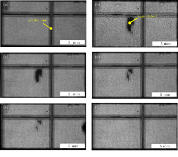
As expected by the above assumption, after several hours, which depends on the size of defect, large defects disappear, and no defect is observed in the c-SAM scanning images. The recovery process is shown in Fig.
 | Fig. 6. Defect recovery processes observed (a) before annealing and cooling, (b) immediately after annealing and cooling, (c) after 38 hours, (d) after 64 hours, (e) after 84 hours, and (f) after 182 hours. |
 | Fig. 7. Interface morphologies of the cross section (a) after annealing and quick cooling and (b) 182 hours later. |
Based on the recovery process of defects, it is concluded that large defects found by the “defect-enlarged approach” result from the combination of micro seams and cracking “weak” bonds. Then the recovery process of “weak” bonds is due to the pressure difference between the atmosphere on the silicon and the high vacuum in the seam. Though micro-defects can be discovered in this work, the underlying physical formation mechanism of the seams in the interfaces needs to be investigated, which is beneficial for controlling the bonding process.
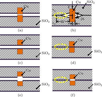
The underlying formation mechanism of the micro-defects is concerned with Cu pad surface topology and the bonding model, which is illustrated in Fig.
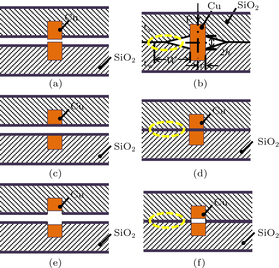 | Fig. 8. Schematic diagrams of surface topology after CMP process of (a) copper in protrusion, (c) flat surface, and (e) copper in dishing. Possible bonding models at the interface of (b) copper in protrusion, (d) flat surface, and (f) copper in dishing. |
 | Fig. 9. Possible cross sectional interface after treatment by “defect-enlarged approach”. |
In this study, the Cu–Cu interconnects with the ultrafine pitches of 6 μm, 8 μm, and 15 μm are implemented by the direct bonding process. A novel effective NDT technology named the “defect-enlarged approach” is proposed to detect micro-defects. It includes an annealing process in an N 2 oven and a quick cooling process in air. After the proposed approach is applied, large defects composed of micro seams and “weak” bonds are found where no defect is detected by traditional c-SAM; these defects disappear in c-SAM images after several hours because “weak” bonds are re-bonded due to the air pressure difference. The underlying physical mechanism originates from the non-homogeneity of Cu surface roughness in the CMP process. In conclusion, the “defect-enlarged approach” is a promising NDT technology for examining the micro-defects in a direct bonding process, and is especially effective in a bonding process with an ultrafine pad pitch of 6 μm. Furthermore, it is significantly important to optimize the CMP process for different bonding processes with different Cu pad pitches, and design rules of Cu pads with a pitch of 6 μm may also be different from those with other pad pitches.
| 1 | |
| 2 | |
| 3 | |
| 4 | |
| 5 | |
| 6 | |
| 7 | |
| 8 | |
| 9 | |
| 10 | |
| 11 | |
| 12 | |
| 13 | |
| 14 | |
| 15 | |
| 16 | |
| 17 | |
| 18 | |
| 19 |