


Domain boundaries in silicene: Density functional theory calculations on electronic properties
[Xiao Hong-Jun, Zhang Li-Zhi, Du Shi-Xuan† , Gao Hong-Jun]
, Gao Hong-Jun]
|
|


†Corresponding author. E-mail: sxdu@iphy.ac.cn
*Project supported by the National Natural Science Foundation of China (Grant Nos. 61390501 and 51325204), the National Basic Research Program of China (Grant Nos. 2011CB808401 and 2011CB921702), and the Tainjin Supercomputing Center, Chinese Academy of Sciences.
By using density functional theory (DFT)-based first-principles calculations, the structural stability and electronic properties for two kinds of silicene domain boundaries, forming along armchair edge and zigzag edge, have been investigated. The results indicate that a linkage of tetragonal and octagonal rings (4|8) appears along the armchair edge, while a linkage of paired pentagonal and octagonal rings (5|5|8) appears along the zigzag edge. Different from graphene, the buckling properties of silicene lead to two mirror symmetrical edges of silicene line-defect. The formation energies indicate that the 5|5|8 domain boundary is more stable than the 4|8 domain boundary. Similar to graphene, the calculated electronic properties show that the 5|5|8 domain boundaries exhibit metallic properties and the 4|8 domain boundaries are half-metal. Both domain boundaries create the perfect one-dimensional (1D) metallic wires. Due to the metallic properties, these two kinds of nanowires can be used to build the silicene-based devices.
Silicene, a two-dimensional (2D) honeycomb lattice of silicon atoms similar to graphene, has attracted tremendous attention owing to its unique physical properties, in particular its Dirac fermion characteristics.[1– 3] Silicene is a prospective candidate for applications in nanotechnology because of its compatibility with existing Si-based semiconductor technologies. Different from the flat honeycomb lattice of graphene, silicene has to be stabilized by a low buckling about 0.44 Å as predicted by density functional theory (DFT) calculation, [4, 5] which enables the band structure to be adjusted more flexibly.[5– 7] Further theoretical studies show that the electronic properties of silicene nano-ribbons and silicene sheets resemble those of graphene, which intrigued fabrication of silicene on different substrates. For example, silicene can be fabricated by means of depositing silicon on Ag (111), [8– 10] Ag (110), [11, 12] Ir (111), [13] and ZrB2 (0001)[14] substrates. Despite recent rapid progress toward creating processible silicene, to date few experimental silicene devices have been reported because of its air unstability issue.[15] Recently, Li et al. have reported the fabrication of a single-layer silicene FET that operates at room temperature.[16] Silicene’ s allotropic affinity with bulk silicon and its low-temperature synthesis compared with graphene and other two-dimensional semiconductors, [17– 19] suggest a more direct integration with current silicon-based semiconductor technology.[20, 21]
However, defects inevitably exist in the experimentally synthesized sheets due to the imperfection of material production processes. Such defects have a strong influence on the electronic, optical, thermal, and mechanical properties of the solid.[22, 23] In fact, many of the characteristics such as the conductance of semiconductors or the mechanical strength and ductility of metals are controlled by defects. Defects in graphene, such as vacancies, adsorption, and doping of foreign atoms open the possibility for tailoring the electronic and magnetic properties of graphene-based structures.[24– 27] Stone– Wales (SW) defects have been predicted to open a band gap in the electronic band structure that can be of potential use in the design of transistors.[28, 29] Several theoretical investigations have been carried out to explain the structure and electronic properties of silicene with defects. Li et al. studied three types of defects of silicene monolayer, and demonstrated that the introduction of single and double silicon adatoms significantly enhances the stability of the system.[30] They also provided the formation energies of several line-defects without any information about the electronic properties. Dong et al. investigated the SW defects in zigzag silicene nanoribbons, and suggested the possibility of tuning the electronic properties using the SW defects.[31] Gao et al. systemically investigated the structures, formation energies, migration behaviors, and electronic/magnetic properties of typical point defects in silicene.[32] However, the electronic properties of the one-dimensional (1D) defects (domain boundaries) in silicene are still not very clear. In this paper, by using density functional theory-based first-principles calculations, we investigated the stability and electronic properties of two kinds of line defects in the free-standing silicene, the 4| 8 defect along the armchair edge and the 5| 5| 8 defect along the zigzag edge. The relative formation energies indicates that 5| 5| 8 domain boundary is more stable than the 4| 8 domain boundary, and the formation energies for both defects are less than 0.15 eV, which is higher than that of the freestanding silicene. Similar to graphene, the electronic properties indicate that the 5| 5| 8 domain boundaries exhibit metallic properties, while the 4| 8 domain boundaries are half-metal.
All geometric relaxation and total energy minimization were carried out using the Vienna ab initio simulation package (VASP).[33] The projector augmented wave (PAW) potentials are used to describe the core electrons and the generalized gradient approximation of Perdew, Burke, and Ernzerhof (PBE) for exchange and correlation.[34] To calculate these two kinds of 1D defect, two models were built. Each model contains two defects (domain boundaries) to keep the mirror symmetry. The two neighboring defects were separated by a ∼ 15-Å defect-free silicene. A vacuum layer of 15 Å was used. The Monkhorst– Pack schemes with 2 × 11× 1 and 2× 15× 1 k-points were used to sample the Brillouin zone for the 5| 5| 8 and 4| 8 defects, respectively. In our calculation, the plane-wave expansion was truncated at a cutoff energy of 300 eV and all Si atoms were relaxed until the net force on every atom was smaller than 0.01 eV/Å . We also define the relative formation energy (eV/atom) of the 1D defect comparing with freestanding silicene by the formula

where Etot is the total energy, Esi is the binding energy per atom in the freestanding silicene, N is the number of total silicon atoms in one unit cell, and n is the number of silicon atoms of 1D defect in one unit, e.g., n = 20 for 5| 5| 8 defect and n = 16 for 4| 8 defect (containing 2 defects in one unit cell).
To form the 1D silicene defect (domain boundary), two key points must be satisfied: 1) two semi-infinite 2D silicene lattice (two domains); 2) a growth fault or a stacking fault of these two domains, where one half of the 2D lattice joins with the other to form the domain boundary. Here, we constructed two kinds of 1D defects. One was the 5| 5| 8 defect, coming from the connection of two zigzag edges (Fig. 1). The other was the 4| 8 defect, coming from the connection of two armchair edges (Fig. 2). Due to the buckling properties of freestanding silicene, silicon atoms in the 1D defect should keep buckling to form the most stable structures, which induce a mirror symmetry (the vertical blue lines in Figs. 3(a) and 3(b)). Figure 1 shows the construction process of a 1D 5| 5| 8 defect in silicene. Firstly, silicene separates into two lattices along the zigzag edge, lattices 1 and 2. Secondly, lattice 2 rotates 180° along X direction. Then two lattices move close with each other along Y direction for 2a (a is the bond length of Si– Si in silicene). Finally, after deleting some overlapped silicon atoms, each of two silicon atoms bond to form the 5| 5| 8 defect. Similar with the 5| 5| 8 defect, the 4| 8 defect can also be constructed by two separated semi-infinite silicene along the armchair edge, which are shown in Fig. 2.
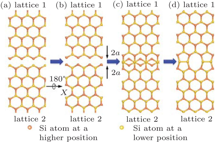 | Fig. 1. Construction of a 5| 5| 8 domain boundary in silicene. (a) Pure silicene lattices 1 and 2. (b) Lattice 2 rotates 180° along X direction. (c) Two lattices move 2a (a is the bond length of Si– Si in silicene) along the direction indicated by the black arrows. (d) Silicene lattice with the 5| 5| 8 domain boundary after the overlapped silicon atoms are deleted. |
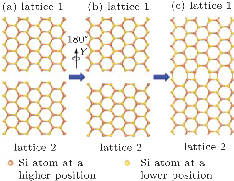 | Fig. 2. Construction of a 4| 8 domain boundary in silicene. (a) Pure silicene lattices 1 and 2 with stacking fault. (b) Lattice 1 rotates 180° along Y direction. (c) Silicene lattice with the 4| 8 domain boundary. |
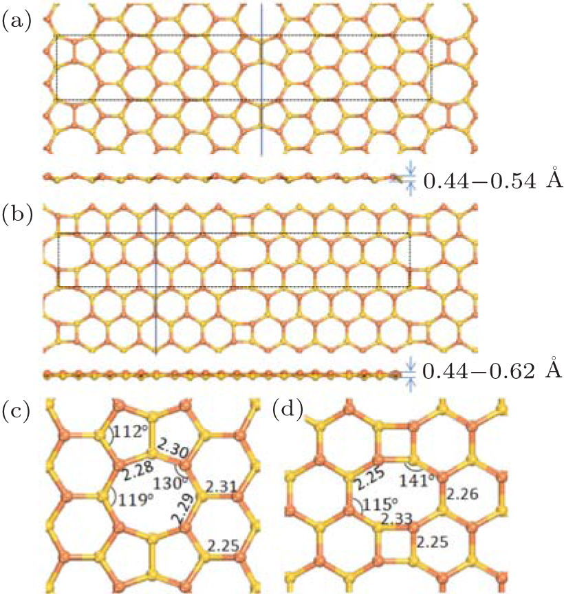 | Fig. 3. Relaxed configurations of the 1D defect structures for the 5| 5| 8 defect (a) and the 1D 4| 8 defect (b), where the black dash rectangles in panels (a) and (b) indicate the supercells used in the calculations, the blue lines indicate the mirror line. The respective buckling distances (in unit Å ) are shown in the bottom of panels (a) and (b). The bond lengths (in unit Å ) and bond angles are shown in panels (c) and (d), which are the zoom-in of panels (a) and (b), respectively. |
Due to the mirror symmetry, the calculation models should contain two mirror symmetrical defects. Figures 3(a) and 3(b) show the relaxed configurations with 5| 5| 8 and 4| 8 defects, respectively. In the black dash square frames, we can find that each supercell contains two mirror symmetric defects separated by zigzag nanoribbon for the 5| 5| 8 defect, and armchair nanoribbon for the 4| 8 defect. The bond lengths (in unit Å ) and bond angles are shown in Figs. 3(c) and 3(d). We can find that the bond lengths are nearly the same as that in freestanding silicene, 2.28 Å . Our calculation results also show that the buckling of these two defects is a little larger than that of the freestanding silicene, which is 0.54 Å for the 5| 5| 8 defect and 0.62 Å for 4| 8 defect, while the buckling in silicene is 0.44 Å .
Then relative formation energies for 5| 5| 8 and 4| 8 defects are 0.07 eV/atom and 0.14 eV/atom, respectively. The 5| 5| 8 defect is more stable than 4| 8 ones, which is in agreement with Li’ s calculation.[30] The relative formation energies for both defects are a little larger than that of the freestanding silicene, which indicate these two defects are not thermodynamically stable. Up to now, silicene can be only growth on the metal substrates, and then, people can construct these 1D defect on the metal surface, similar with the graphene 5| 5| 8 defect on Ni (111) surface.[27] Recently, experimental results show that silicene growing on Ag (111) substrate can be transferred on SiO2 substrate, [16] suggesting that 1D silicene defect could also be grown on metal surface and then transferred on other substrate.
The electronic properties of the 5| 5| 8 defect are shown in Fig. 4. According to its band structures in Fig. 4(a), two almost flat bands appear around the Fermi level, which is similar to that of the 5| 5| 8 defect in graphene.[27] It indicates the metallic properties of the silicene 5| 5| 8 defect. The projected density of states (PDOS) in the right part in Fig. 4(a) shows a sharp peak around the Fermi level, which correspond to the flat bands of the band structures. Comparing with the half metal properties of freestanding silicene (the DOS is shown with the black dash line in the right parts of Fig. 4(a)), this silicene supercell with 5| 5| 8 defect exhibits metallic properties. From the charge density distributions around the Fermi level (as shown in Fig. 4(b)), it can be found that nearly all charges are assembled along the 5| 5| 8 defect, which indicates that the metallic property does come from the 1D defect. Therefore, a perfect 1D metallic wire in a 2D half metal layer is constructed. As shown in Fig. 4(b), we find that the charge density distributes inhomogeneously on different Si atoms. The charge density only distributes along the 1D 5| 5| 8 defect. It is found that the charge tends to distribute at the dangling bonds, the top of the Si atoms at a higher position, and the bottom of the Si atoms at a lower position (Fig. 4(b)), with a slight difference. The difference comes from the slightly different sp2– sp3 hybridization of the silicon atoms at the defect. The sp3 hybridization induces the buckling of silicene. The localization of the electronic states at the defect indicates that the 5| 5| 8 defect is a perfect 1D metallic wire embedded in the 2D silicene, which suggests that the silicene-based electronic device can be connected by the 5| 5| 8 defect.
 | Fig. 4. Electronic structures of the 1D 5| 5| 8 silicene defect. (a) The band structures and the density of states of the perfect silicene and the 1D 5| 5| 8 silicene defect. (b) Charge density distributions around the Fermi level (− 0.2 eV ∼ + 0.2 eV iso-surface = 0.01 e/Å 3), top view and side view. |
For the defect formed along the armchair edge, the electronic properties of 4| 8 defect are different from that of 5| 5| 8 defect. In Fig. 5, we provide the electronic structures of 4| 8 silicene defect. The band structure (Fig. (5a)) shows that there is a crossing point at the Fermi level. The DOS for the 1D 4| 8 defect exhibits a minimum point at the Fermi level, which is similar to that of a freestanding silicene (right panel in Fig. 5(a)). It means that the 1D 4| 8 defect exhibits half-metal properties. We know that most of the silicene armchair nanoribbons are semiconductor. But the 1D 4| 8 defect formed at the silicnene armchair edge exhibits half-metal properties. The half-metal properties of the 4| 8 defect are the same as the freestanding silicene and both Dirac cones reveal nearly the same Fermi velocities. Therefore, the 1D 4| 8 defect could be constructed to connect the silicone-based electronic devices. Similar to graphene, the electronic states of silicene around the Fermi level mainly come from the pz orbitals, the honeycomb configuration determines that the valance and conduction bands are symmetric. For these two defects, mirror symmetry also exists (Figs. 3(a) and 3(b)), which results in the symmetry of pz bands. The charge density distributions (Figs. 5(b) and 5(c)) for the lowest conduction band (yellow) and highest valance band (blue) reveal that both charge density plots at the Dirac points are nearly the same as those in silicene. Similar to 5| 5| 8 defect, the charge density distributes inhomogeneously on different Si atoms and only distributes along the 1D 4| 8 defect. The sp2 hybridization of the four-membered ring contributes a lot on both the valence band and conduction band because the buckling of the four-membered ring is the lowest one (0.44 Å ). For the atoms on the common bond of six-membered ring and eight-membered ring, the sp3 hybridization dominates and the charge tends to distribute at the dangling bonds because of the higher buckling.
 | Fig. 5. Electronic structures of the 1D 4| 8 silicene defect. (a) The band structures and the density of states of the perfect silicene and the 1D 4| 8 silicene defect. (b) Charge density distributions for the lowest conduction band, top view and side view, (c) charge density distributions for the highest valance band, top view and side view (iso-surface = 0.005 e/Å 3). |
By using first-principles calculations, two kinds of 1D defects in the free-standing silicene, the 4| 8 defect along the armchair edge and the 5| 5| 8 defect along the zigzag edge, have been investigated. The constructions of these two 1D defects are investigated and we can get these two defects by connecting the armchair/zigzag edges of the semi-infinite 2D silicene. Comparing their relative formation energies with that of silicene, it can be found that the 5| 5| 8 defect is more stable than the 4| 8 defect. Similar to graphene, the electronic properties reveal that the 5| 5| 8 domain boundaries exhibit metallic properties, while the 4| 8 domain boundaries are half-metal. Due to their metallic and half-metalic properties, these two kinds of defects can be used to build the all-silicene devices.
| 1 |
|
| 2 |
|
| 3 |
|
| 4 |
|
| 5 |
|
| 6 |
|
| 7 |
|
| 8 |
|
| 9 |
|
| 10 |
|
| 11 |
|
| 12 |
|
| 13 |
|
| 14 |
|
| 15 |
|
| 16 |
|
| 17 |
|
| 18 |
|
| 19 |
|
| 20 |
|
| 21 |
|
| 22 |
|
| 23 |
|
| 24 |
|
| 25 |
|
| 26 |
|
| 27 |
|
| 28 |
|
| 29 |
|
| 30 |
|
| 31 |
|
| 32 |
|
| 33 |
|
| 34 |
|