


Silicene: from monolayer to multilayer — A concise review
[Li Hui† , Hui-Xia Fu, Meng Sheng]
, Hui-Xia Fu, Meng Sheng]
|
|


†Corresponding author. E-mail: huili8@iphy.ac.cn
*
Silicene, a newly isolated silicon allotrope with a two-dimensional (2D) honeycomb lattice structure, is predicted to have electronic properties similar to those of graphene, including the existence of signature Dirac fermions. Furthermore, the strong spin–orbit interaction of Si atoms potentially makes silicene an experimentally accessible 2D topological insulator. Since 2012, silicene films have been experimentally synthesized on Ag (111) and other substrates, motivating a burst of research on silicene. We and collaborators have employed STM investigations and first principles calculations to intensively study the structure and electronic properties of silicene films on Ag (111), including monolayer, bilayer, and multilayer silicenes, as well as hydrogenation of silicene.
Graphene, a slice of sp2-bonded carbon film from bulk graphite, has brought a storm of discoveries about two-dimensional (2D) materials in the last decade in the fields of physics, chemistry, and material science, due to graphene’ s unique Dirac-type electronic structure and outstanding properties such as high thermal and electrical conductivity, mechanical stability, and inert chemical reactivity.[1] Beyond graphene, people are searching for other elemental 2D materials. One attractive material is silicene, the one-atom-thick silicon film with a honeycomb lattice, first predicted based on first principles calculation.[2] Free-standing silicene adopts a low-buckled 2D structure with a buckling distance of ∼ 0.4 Å . As silicene is the silicon analog of graphene, many properties of graphene have been predicted also to exist for silicene, including the signature Dirac fermions. Furthermore, the predicted relativistic Dirac fermions, which are due to spin orbital coupling (SOC) being stronger in silicon than in carbon, would make single-layer silicene (SLS) a potential 2D topological insulator, expected to yield an observable spin quantum-Hall effect.[3, 4] Multilayer silicene (MLS) films also demonstrate interesting electronic properties, such as chiral superconducting behavior, [5] valley-polarized quantum Hall effect, [6] and electronic structure that is dramatically tunable by varying stacking modes.[7, 8] It is also commonly proposed that silicene is more compatible with silicon-based industry.
Within the past three years, great progress has also been made in the field of experimental synthesis of silicone.[9– 29] Unlike graphene, which can be exfoliated from van der Waals (vdW)-packed graphite, sp2-hybridized silicon does not exist in nature. Thus, silicene can be achieved only by stabilizing interfacial interaction with a substrate. So far, although growth if monolayer silicon film has been reported on several substrates such as ZrB2, [11] Ir (111), [12] and Ag (110), [23] more than 90% of the research reports on silicene focus on silicene epitaxially grown on Ag (111) surface.[9, 10, 13– 22] Both SLS and MLS have been grown on Ag (111) surface using molecular beam epitaxy (MBE) and intensively studied by scanning tunneling microscopy (STM) and angle-resolved photoemission spectroscopy (ARPES), combined with first principles calculations. However, the atomic structure of silicene on Ag (111) is still under heavy debate, because it has been found that SLS can assume numerous metastable structures on Ag (111), depending on growth temperature and dynamics, such as 3× 3, 


On the other hand, silicon atoms in silicene have partial sp3-hybridization, displaying much higher reactivity than purely sp2-hybridized carbon atoms in graphene. Thus, silicene is easier to dope with other atoms, which can dramatically modify the electronic properties.[30– 34] For example, first principles calculations predict that hydrogenation can open a large band gap (∼ 3 eV) for silicone, [30] and that halide-doped silicene can be a large-gap 2D topological insulator. Recent experiment has confirmed silicene is much easier to be hydrogenated than grapheme.[34] The doped silicene also launches a new field for making electronic devices based on silicene.
In this review, we will introduce previous theoretical predictions of the structure of silicene (Section 2), the recent development of SLS and MLS grown on Ag (111) surface and other substrates (Section 3), as well as some of the newest results on hydrogenated silicene (Section 4).
The properties of free-standing monolayer silicene were first predicted using first principles calculations in the framework of density functional theory (DFT) by Ciraci et al. in 2009, [2] and even before that, monolayer silicon layer had already been theoretically studied.[35] As shown in the potential energy surface (PES) plot as a function of the lattice constant (Fig. 1(c)), three local energy minima can be obtained for monolayer silicon honeycomb sheet, the high-buckled (HB), the low-buckled (LB), as well as the planar (PL) structures. The HB structure is closer to a bilayer silicon film. According to the phonon calculation and finite temperature molecular dynamics (MD) simulation, the PL structure can spontaneously transform to the LB structure, and the LB silicene is thermodynamically stable. Thus, the LB structure of silicon, now called silicene, can theoretically exist. As shown in Figs. 1(a) and 1(b), the optimized lattice constant of free-standing silicene is 0.387 nm, and the buckling depth is ∼ 0.4 Å based on our DFT calculations. The band structure (Fig. 1(d)) demonstrates a linear dispersive Dirac cone at the K points in the first Brillouin zone of silicene.
 | Fig. 1. (a) The side and (b) top view of free-standing low-buckled silicene obtained from DFT calculation. (c) The potential energy surface (PES) of silicene versus lattice constant. (d) The calculated band structure of low-buckled silicene. |
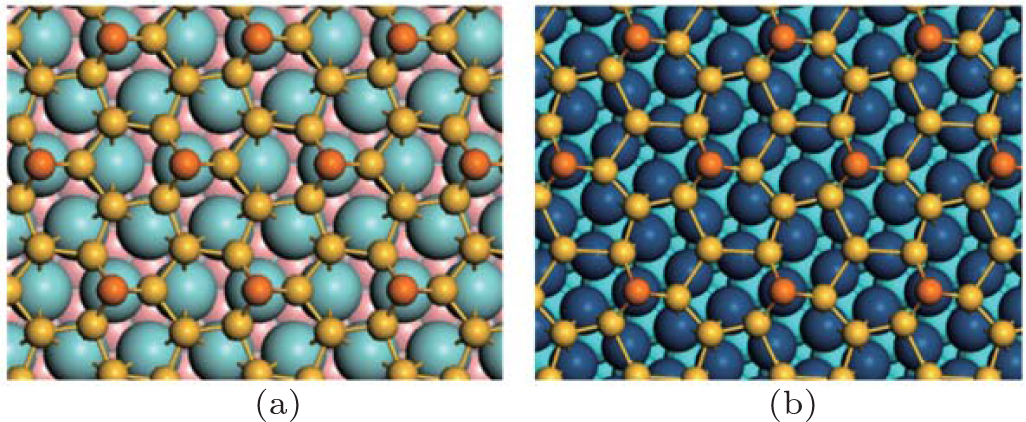
The details of isolated SLS are now well known, but despite great efforts in the last decade to explore the atomic and electronic structures of bilayer silicon (BLS) films, these structures remain unclear.[36] For example, the widely used BLS model is the AB (Bernal) stacked model; however, using first principles calculation, Zeng et al. predicted a planar covalent-bonded silicon bilayer with AA-stacking mode, [8] Morishita et al. reported a re-DL-Si morphology from reconstruction of two-layer Si (111) surface, [37] and Xiang et al. predicted an Si-Cmme quasi-bilayer structure, using global optimization.[38] It is well known that both interlayer interaction and stacking order play key roles in determining the properties of multilayer silicene. Unlike van der Waals stacking in bilayer graphene, whose global minimum is AB-stacked, BLS has been proposed to have various morphologies due to complicated interlayer covalent bonds.[39]
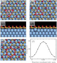
We employed a method similar to that used for studying SLS to search for stable and functional BLS based on DFT calculations.[7] The PBE functional[40] was employed for structural research of BLS, and the HSE functional[41] was used for electronic structure calculation. The projector augmented wave (PAW) pseudopotentials combined with plane-wave basis set (energy cutoff at 250 eV) were used with the Vienna ab initio Simulation Package (VASP).[42] By scanning the PES of bilayer silicon sheets related to the lattice constant and starting with AA and AB stacking modes (Fig. 2(e)), several metastable configurations of BLS have been found, which are named by the combination of stacking mode and the order of cohesive energies. Among these minima, the most stable BLS morphology, 1AA, is the previously predicted planar AA-stacking BLS (Fig. 2(a)). The most stable AB-stacking BLS, 1AB is the widely used BLS model (Fig. 2(b)). We also found a vdW-packed BLS isomer, 2AA (Fig. 2(c)), which has energy comparable to that of 1AB. According to MD simulation, we further found a new stable structure of BLS, in which the two silicene layers are slightly staggered with respect to each other, and we named the structure slide-2AA.
Although the cohesive energies of these BLS morphologies are not much different, they demonstrate a variety of distinct electronic properties. The calculations show that the 2AA isomer has a semimetal electronic structure, in which the energy gap is 0, but the density of state (DOS) is also 0 at the Fermi level. The stable structure of BLS in our calculations, slide-2AA, is a semiconductor with a significant band gap of 1.16 eV (HSE level), while all the other morphologies of BLS are metallic or semimetallic. It is further found that the transition barriers between 2AA, 1AB, and slide-2AA (∼ 29 meV/Si) are very close to the interlayer sliding barrier of graphite, [43] indicating we can easily change the stacking mode of BLS, thereby tuning their electronic properties. The unique relationship of structure and electronic properties in BLS has profound implications for nanoelectronic and electromechanical devices.
 | Fig. 2. Upper panels: Top and side views of (a) 1AA, (b) 1AB, (c) 2AA, and (d) slide-2AA structures of BLS. Lower panel (e): Cohesive energy (PBE level) versus lattice constant for AA (blue line) and AB (red line) stacking modes. The labels 1, 2, 3 in blue and red fonts denote each of three minima found for AA and AB modes, respectively. The cohesive energy of slide-2AA versus lattice constant (cyan short curve) is also shown.[7] |
As the sp2-hybridized Si is not stable in nature, the only way to synthesize silicene is to grow it on substrates in vacuum. Growth of SLS on Ag (111) by MBE was first reported by Aufray et al. in 2010.[44] However, the results claimed in this work are seriously doubted, since the measured lattice constant of the honeycomb structure in their STM image is 17% shorter than the predicted lattice constant of free-standing silicene. In the same year, fabrication of silicene nanoribbons on Ag (110) surface was also reported by Le Lay et al.[23] People usually choose silver as the supporting substrate for silicene because silver cannot form an alloy with silicon.
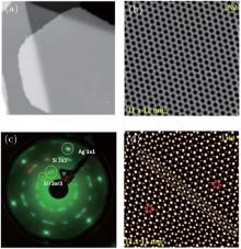
In 2012, the dynamics for growth of SLS on Ag (111) were convincingly studied independently by both Wu et al.[10] and Le Lay et al.[14] The experiments were performed in an ultra-high-vacuum (UHV) chamber combined with a home-made low-temperature STM. Silicon was evaporated from a heated Si wafer with a deposition flux onto a single-crystal Ag (111) substrate. The STM observations were performed at liquid nitrogen temperature (77 K) and liquid helium temperature (4 K) with chemically etched tungsten tips. All the STM data were recorded in the constant-current mode. The differential conductance (dI/dV) maps were extracted from the lock-in signal by applying a modulation of 20 mV at 777 Hz to the tip bias. By carefully changing the temperature of substrate and the amount of deposited Si atoms, the phase diagram of silicene growth on Ag (111) was obtained. As shown in Fig. 3(d), the Si atoms form clusters below 400 K, and form several metastable reconstructed surfaces strongly bonded to the substrate: in the range from 400 K to 530 K, the 


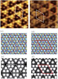
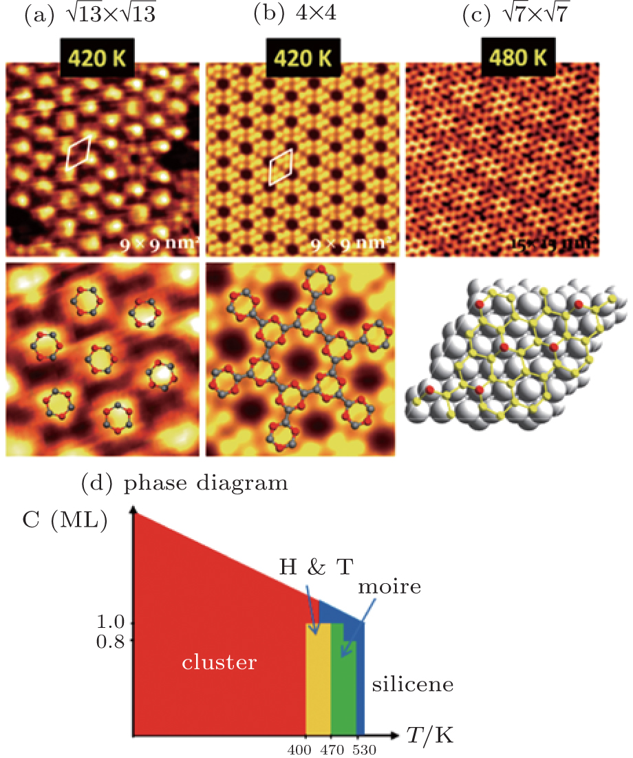 | Fig. 3. Large scale (upper panels) and high resolution (lower panels) STM images of (a)   |
Unlike the metastable silicon layer mentioned before, in which silicon atoms are strongly bonded to silver, the SLS formed at high temperature has very different structural properties, [9] such as a constant height of 0.26 nm and a linear dispersive surface state, which will be discussed in the following sections. As shown in Fig. 4(a), large scale SLS films were obtained, which exhibit perfect layered structure and continuously cover the different height stages of the substrate. A high resolution STM image shows that this silicon film has the same honeycomb structure (Fig. 4(b)) as DFT-predicted silicene; however, its lattice constant (0.67 nm) is 


 | Fig. 4. (a) Large scale and (b) high resolution STM images of    |
In order to understand the observed 
After trying various prototype supercells to model epitaxial silicene, a reasonable atomic model of 


The scanned transition barrier for these two mirror-symmetrical 

 | Fig. 5. Top views [(a) and (b)] and side views [(c) and (d)] of two mirror-symmetrical    |
The most attractive property of silicene is its novel electronic properties, especially its potential to support linear dispersive Dirac fermions like those of grapheme.[2] In addition, measuring the characteristic electronic structure of SLS provides further proof of the proposed silicene model on Ag (111). Thus, the electronic structure of SLS on Ag (111) has been intensively studied by both experiments and calculations. However, there are still debates on whether SLS can sustain electronic properties comparable to those of free-standing silicene, due to the Si– Ag interaction.[11, 46– 48]
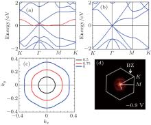
One way to probe the Dirac-type electrons is to investigate the quasiparticle interference (QPI) pattern based on STS.[18, 21] For example, the constant energy contours (CECs) in reciprocal space around the Dirac cone form small circles centered at the high symmetry K points; therefore, free carriers are scattered both within the small circles (intravalley scattering) and between circles (intervalley scattering), resulting in unique QPI patterns in real space. Similar QPI patterns have been observed for 


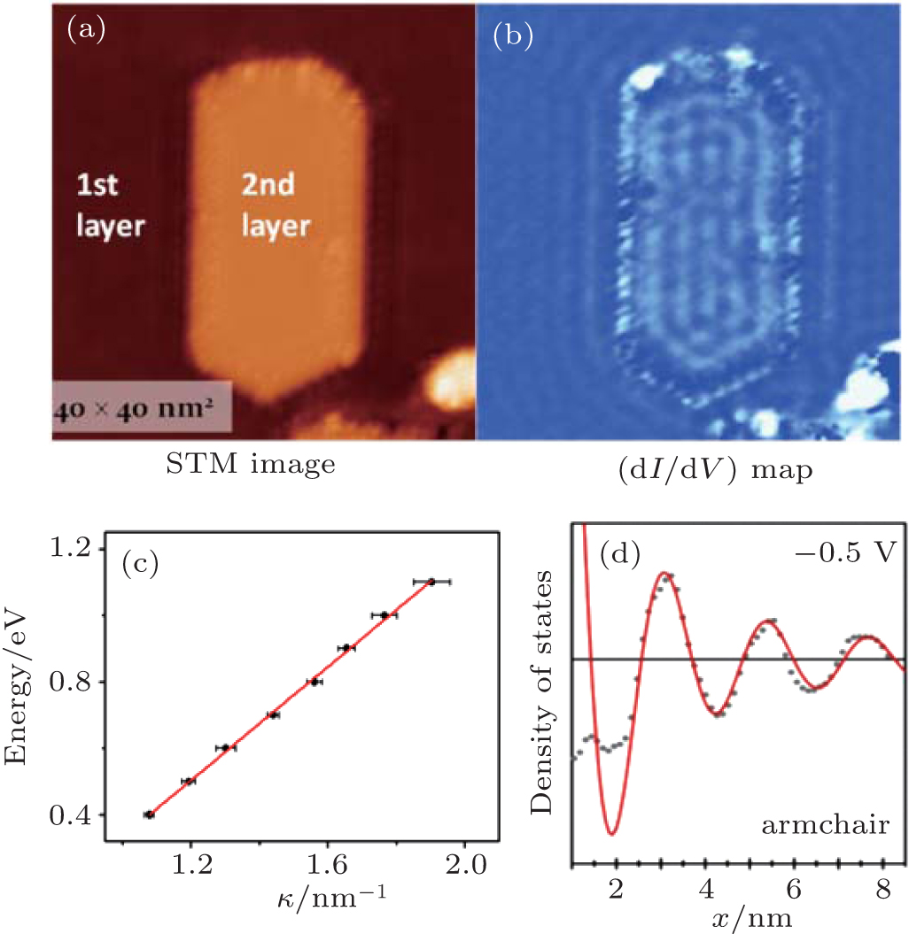 | Fig. 6. (a) STM image (40 nm× 40 nm) of SLS surface containing an island of BLS, taken at tip bias – 1.0 V. (b) dI/dV map of the same area as panel (a), taken at tip bias of 0.5 V. (c) Energy dispersion as a function of κ for silicene, determined from the wavelength of QPI patterns. (d) LDOS on SLS as a function of distance from armchair edges at – 0.5 V. The position of step edge is set at x = 0. Gray dots, experimental values; red lines, fits to the data.[9, 21] |
The Dirac cone in the band structure of distorted 


 | Fig. 7. (a) and (b) Band structures of the   |
SLS has also been grown on substrates other than silver. For example, experimental evidence for epitaxial SLS on ZrB2 (0001) thin film and the Ir (111) surface was reported by Yamada-Takamura et al., [11] and Gao et al., [12] respectively. It is interesting that SLS films on both these substrates also adopt 


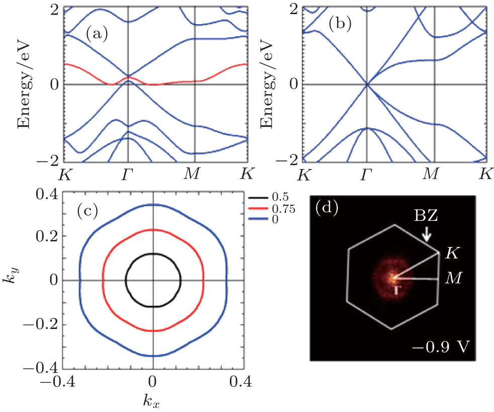
Beyond SLS, MLS has also been studied on Ag (111).[22, 24– 29] As shown in Fig. 6(a), the multilayer silicene islands always exist on synthesized SLS. Recent experiments show MLS on Ag (111) can grow in a layer-by-layer fashion up to ∼ 50 layers (L) or more.[22] Unlike various metastable morphologies of SLS on Ag (111), MLS always assumes a unique 

The experimental method for studying MLS was the same as in the SLS study. Consistent with other reports, our STM images show that MLS samples always adopt a 
Similar to our STS analysis of SLS, we probed the electronic structure of MLS using QPI. The standing wave can be seen in the typical dI/dV map of MLS shown in Fig. 9(e). It is interesting that a linear quasiparticle energy– momentum dispersion relation is obtained from the dI/dV maps at various energy ranges, as shown in Fig. 9(f), indicating that MLS has linear dispersive bands similar to those of SLS. This result contradicts our previous findings that the Dirac-type electrons exist only for free-standing monolayer silicene.
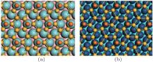
 | Fig. 9. (a) STM image (Vtip = 1.2 V) of coexisting SLS, BLS, and trilayer silicene films. (b) and (c) High resolution STM images of area labeled by white squares in panel (a). The atomic structure of the  |
To understand the experimentally observed 
In the calculation, the MLS is initially van der Waals packed, but during the optimization process it spontaneously forms interlayer covalent bonds leading to a diamond bulk structure; at the same time, a 

It is interesting that the 


We further calculate the band structure respectively projected to MLS and Ag (111) for MLS/Ag (111). As shown in Fig. 10(c), a cone-like surface state is found near the Fermi level for MLS. Such a cone-like surface state can provide MLS the signature Dirac-type electrons, which can be observed by both STS and ARPES. The Fermi velocity obtained from the slope of this surface state is in close agreement with the previous ARPES measurement.[24] Analysis shows that most Si atoms in flat-lying positions have formed delocalized π bonds leading to a Dirac band structure. It should be mentioned that another cross of linear bands is also clearly observed for Ag (111) substrate (Fig. 10(d)), which is the effect of band folding of bulk Ag (111) in the Brillouin zone of the 
 | Fig. 10. (a) Side view of 5-layer MSL on Ag (111) based on DFT calculation. (b) Side view of free-standing 5-layer MSL thin film. The electronic band structure is projected onto (c) MLS and (d) Ag (111) substrates, respectively. The size of dots corresponds to the weight of the contribution. |
It is known that conventional bulk Si (111) surfaces obtained from traditional treatments always forms drastic reconstructions, including 2× 1, 5× 5, and the complicated dimer-adatom-stacking fault (DAS) configuration of Si (111)-7× 7. These reconstructions are accompanied by serious bond breaking/reforming to saturate dangling bonds.[53– 59] On the other hand, the morphology of MLS grown at much lower temperatures represents a new bottom-up approach to obtaining an ideal Si (111)-1× 1 surface that preserves the original hexagonal bond topology and holds a Dirac-type surface state. In addition, recent work has found that MLS is robust in air, [26] which greatly increases the potential for its practical application. The study of MLS provides new fundamental understanding of silicon and encourages hope for the future development of Si-compatible devices.
Due to the potential application of graphene as hydrogen storage material, and a requirement of modification for obtaining the zero-gap electronic structure, hydrogenation of graphene has been widely studied in recent years.[60] As mentioned before, Si atoms in silicene are partially sp3-hybridized, giving silicene stronger reactivity than pure sp2-hybridized graphene. As a result, silicene should be easier to hydrogenate. Pioneering theoretical work on freestanding H-doped silicene showed that hydrogenation can bring significant modifications to silicene, such as large band gap, [30] ferromagneticity, [32] and optoelectronic properties.[33] Recently, with our collaborators, we did the first-ever STM experiment combined with first principles calculations on the hydrogenation of SLS on Ag (111).[34]
The experiments were based on the 3× 3 SLS (with respect to the Si (111)-1× 1 lattice) on Ag (111) grown using the method mentioned before, as this silicene phase is the simplest and most well understood. The SLS surface at room temperature was then exposed to dissociated H2 gas from a hot tungsten filament. The calculation details are also the same as the computational method described before.
High resolution STM images reveal that the hydrogenated 3× 3 SLS/Ag (111) has two kinds of hydrogenation pattern: 7H-adsorption and 6H-adsorption, as respectively shown in Figs. 11(a) and 11(b), indicating that the SLS is not fully hydrogenation-saturated. The coexistence of different hydrogenation patterns can be found in Fig. 11(b). This phenomenon can be explained by the lateral shift of SLS or the change of buckling Si atoms after hydrogenation. The first-principles calculations give the exact models for both hydrogenation patterns, as respectively illustrated in Figs. 11(c) and 11(d). The simulated STM images for both hydrogen adsorption modes (Figs. 11(e) and 11(f)) closely agree with the experimental STM images. Coverage in Fig. 11(d) is higher than in Fig. 11(c), implying that hydrogenated silicene prefers to adopt the latter structure in a hydrogen atmosphere. This is consistent with the experimental observation that most hydrogenation patterns are the same as that in Fig. 11(a). The binding energy of H atoms for the two configurations also shows that the hydrogenated 3× 3 SLS with 7H atoms in one unit cell is more stable. It is noted that the predicted band gap of free-standing H-silicene was not observed, due to the Si– Ag interaction.
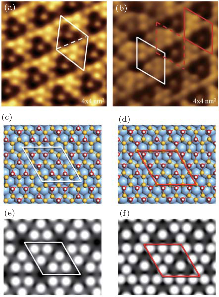 | Fig. 11. (a) STM image of 7H-hydrogenated 3× 3 SLS/Ag (111). The white rhombus marks a unit cell of the structure. (b) Coexistence of 7H-hydrogenated (red cell) and 6H-hydrogenated (white cell) SLS. The structural models of (c) 6H-hydrogenated and (d) 7H-hydrogenated SLS from DFT optimizations; corresponding simulated STM images are shown in panels (e) and (f), respectively.[34] |
Another important feature of hydrogenated 3× 3 SLS is reversible dehydrogenation. Fully hydrogenated SLS can be completely restored to its original state by increasing the temperature to ∼ 450 K. Such easily reversible hydrogenation suggests that silicene could be used for hydrogen storage. Our work on silicene hydrogenation has pioneered the area, enabling further investigation of the electronic properties of hydrogenated silicene.
In this review, we have summarized some experiment and theoretical studies of silicene, mainly work done by us and our collaborators since 2012. We introduced three areas of silicene research: pure theoretical prediction of configurations and electronic properties of SLS and BLS, combined experimental-theoretical studies of SLS and MLS, and hydrogenated SLS on Ag (111) substrate. Free-standing silicene is theoretically predicted to have a simple 2D honeycomb structure and signature Dirac bands. However, according to the work reviewed here, it is found that SLS on Ag (111) is an extremely complex system. For MLS, the stacking style of silicene layers makes the system even more complicated. Thus, to figure out the atomic and electronic structure of silicene/Ag (111) is much more difficult than we expected when we started looking into the subject. Even though the highest resolution STM observation and extensive first principles calculations were employed, we can only propose some reasonable models and explanations of such systems. So nowadays, the structure and electronic properties of silicene on Ag (111) are still under debate.
Our studies demonstrate that, among all the metastable phases of SLS on Ag (111), the 


Finally, although silicene systems have been intensively studied during these years, this is still just the beginning of silicene research. As we mentioned, the model of silicene on Ag (111) is still under debate. The main reason is that Si– Ag interaction is quite strong, which may seriously interfere with the electronic properties of silicene adsorbed on it. Furthermore, because the metallic properties of Ag can overwhelm the electronic properties of silicene, it is difficult to distinguish information about electrons of silicene from that about substrate electrons. Therefore, to grow silicene on a weakly interacting semiconductor substrate is the most urgent task for future study of silicene. In addition, since silicene is easier to functionalize than graphene, using different elements to dope silicene can be another important subject in the coming years.
| 1 |
|
| 2 |
|
| 3 |
|
| 4 |
|
| 5 |
|
| 6 |
|
| 7 |
|
| 8 |
|
| 9 |
|
| 10 |
|
| 11 |
|
| 12 |
|
| 13 |
|
| 14 |
|
| 15 |
|
| 16 |
|
| 17 |
|
| 18 |
|
| 19 |
|
| 20 |
|
| 21 |
|
| 22 |
|
| 23 |
|
| 24 |
|
| 25 |
|
| 26 |
|
| 27 |
|
| 28 |
|
| 29 |
|
| 30 |
|
| 31 |
|
| 32 |
|
| 33 |
|
| 34 |
|
| 35 |
|
| 36 |
|
| 37 |
|
| 38 |
|
| 39 |
|
| 40 |
|
| 41 |
|
| 42 |
|
| 43 |
|
| 44 |
|
| 45 |
|
| 46 |
|
| 47 |
|
| 48 |
|
| 49 |
|
| 50 |
|
| 51 |
|
| 52 |
|
| 53 |
|
| 54 |
|
| 55 |
|
| 56 |
|
| 57 |
|
| 58 |
|
| 59 |
|
| 60 |
|