Improved performance of microcrystalline silicon solar cell with graded-band-gap silicon oxide buffer layer
Hebei Key Laboratory of Optic–Electronic Information Material, College of Physics Science and Technology, Hebei University, Baoding 071002, China
†Corresponding author. E-mail: hbuyuwei@126.com
‡Corresponding author. E-mail: laser@hbu.edu.cn
*Project supported by the Key Basic Research Project of Hebei Province, China (Grant Nos. 12963930D and 12963929D), the Natural Science Foundation of Hebei Province, China (Grant Nos. F2013201250 and E2012201059), and the Science and Technology Research Projects of the Education Department of Hebei Province, China (Grant No. ZH2012030).
1. IntroductionIn recent years, the p-type hydrogenated microcrystalline silicon oxide (p-μ c-SiOx:H) material is widely used in thin film silicon solar cells as a window layers because of its advantages such as low absorption, low refractive index, and tunable resistance.[1] It is a mixture phase material which contains oxygen-rich (O-rich) phase and silicon-rich (Si-rich) phase.[2] So far, researchers have succeeded in controlling the incorporated oxygen content in this material to meet the requirements for the window layer.[3] The incorporation of oxygen significantly increases the band gap of the p-μ c-SiOx:H compared with the intrinsic layer and improves its short wavelength response.[4– 6] However, it inevitably leads to the mismatch of band gap which introduces p/i interface barrier reducing carriers extracting.[7] In addition, during the intrinsic layer growth, the deep level interface defects formed by its incubation and the boron diffusion from p-layer cause the carrier recombination rate to increase near the p/i interface.[8, 9] Inserting buffer layer into p/i interface is a common means to resolve the above problems in the thin film solar cells. Introducing a μ c-SiOx:H buffer layer into p/i interface facilitates the nucleation of the subsequent intrinsic μ c-Si:H layer. A gain in short-circuit current density and an increase of open-circuit voltage have been observed, which results from the dramatically reducing density of interface defects.[10] Therefore, further work is still needed to reduce the band gap mismatch between the p-layer and i-layer for improving the carrier transport through the p/i interface.
In this study, the graded band gap silicon oxide buffer layer is introduced at p/i interface and its effects on cell performance are investigated. To better understand the effects of the buffer on material microstructure of the intrinsic layer, the Raman spectroscopy spectrum is directly measured on the cells with different excitation wavelengths. The densities of interface defects are obtained through the capacitance– voltage (C– V) measurements. The J– V results show that the S-shape curve is removed after introducing the graded buffer layer and the cell performance is significantly improved.
2. ExperimentHydrogen (H2) and silane (SiH4) mixture was used as a source gas to prepare the intrinsic absorb layer. The H2 diluted trimethylboron (TMB, 2% ) and phosphine (PH3, 0.5% ) were added to obtain p-type and n-type doped layer, respectively. The H2 diluted carbon dioxide (CO2, 10% ) was employed as an oxygen source. The p-μ c-SiOx:H film was deposited at 150 ° C by radio frequency (13.56 MHz) plasma enhanced chemical vapor deposition (PECVD) in a multi-chamber system and the plasma power density was 0.082 W/cm2. The flow rates of SiH4, H2, TMB, and CO2 were 1, 200, 0.5, and 1 sccm, respectively.
At the end of the p-μ c-SiOx:H layer deposition process, the flow of the TMB was set to be zero and the CO2 was gradually reduced to zero for 4 min at a uniform rate for the buffer layer to grow. The estimated buffer layer thickness was about 4 nm.
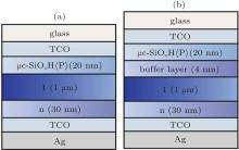
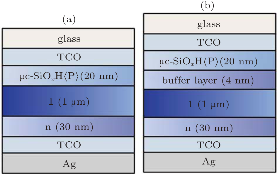
Solar cells with p– i– n structure deposition sequence were prepared on AZO (ZnO:Al) coated glass substrates. The device structures without and with buffer layer are referred to as cell A and cell B, respectively. The area of each cell is 0.25 cm2. The structures of cell A and cell B are shown in Fig. 1.
The film thickness was measured using a step profiler (DeKtaK XT). The structural properties were characterized with Raman spectroscopy (LabRAM HR Evolution, including 325 nm, 532 nm, and 633 nm wavelength lasers). The solar cell performance was characterized by the measurements of current density versus voltage (J– V) under an AM 1.5 solar simulator at 25 ° C. The spectral responses of the cells were obtained from external quantum efficiency (EQE) measurements. The C– V measurements were obtained by using B1500A semiconductor device parameter analyzer.
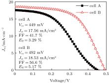
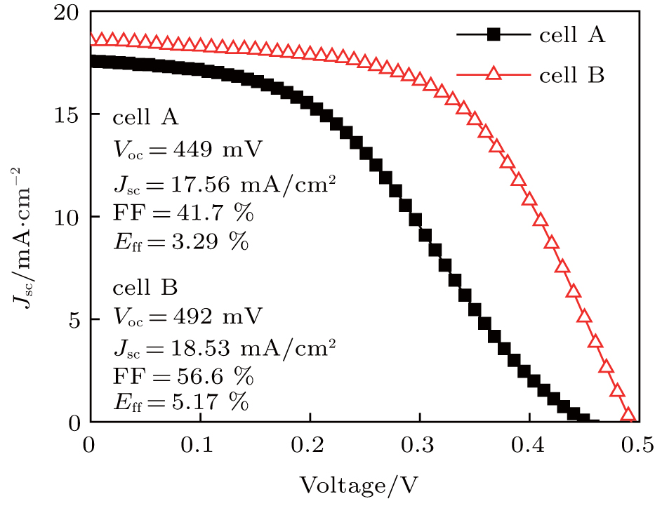
3. ResultsFigure 2 shows the J– V curves of the the μ c-Si:H solar cells. The J– V characteristic of cell A exhibits S-shape, which indicates that there is a barrier preventing the extraction of holes at p/i interface, leading to low values of the open-circuit voltage (Voc), the short-circuit current density (Jsc), and the fill factor (FF). Compared with cell A, cell B with graded buffer layer exhibits improved performance indicating that the p/i interface barrier is reduced.
The J– V characteristics of the cells obtained under dark conditions are used to analyze the contributions of the buffer layer on Voc. The J0 and n can be obtained by the following diode equation:

where J0 is the saturation current density, q is the electric charge, n is the diode quality factor, k is the Boltzmann’ s constant, and T is the absolute temperature. Similar n values are obtained to be 1.6 and 1.65 for the cell A and cell B, respectively. Compared with the J0 (1.06 × 10− 10 mA/cm2) of cell A, the J0 of cell B is low (3.90 × 10− 11 mA/cm2), indicating that the introduction of buffer layer reduces carrier recombination at p/i interface.
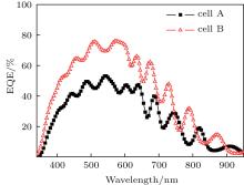
Figure 3 shows the curves of EQE versus wavelength of the cells A and B. A remarkable improvement in the short wavelength region is observed in cell B. Since the short wavelength light will be nearly fully absorbed in the front part of i-layer near p/i interface, the improved response in the blue region should be attributed to the reduced defective region at p/i interface.
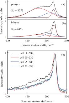
To analyze the effects of the buffer layer added on the microstructure of i-layer, Raman measurements were performed on the single layer and on the device. Figures 4(a) and 4(b) show the Raman spectra of p- and i-layer deposited on the glass, respectively. The crystallized volume fraction (Xc) is evaluated using Xc = (I510 + I520)/(I480 + I510 + I520), where Im denotes an integrated intensity in units of m cm− 1.[11] The obtained values of Xc in p- and i-layer are 32 % and 54 % , respectively. For the i-layer grown on the p-layer, the increase in crystallinity from p- to i-layer inevitably involves a higher volume of amorphous in the initial i-layer, and a suitable buffer layer will be needed for obtaining an improved structure near the p/i interface.
Figure 4(c) shows the Raman spectra of the two solar cells excited with a green (532 nm) laser and a red (633 nm) laser from p-layer side, respectively. The green light is used for probing the microstructures of the top layer near the p/i interface, while the red light for that of the bulk i-layer.[12] A comparison between cell B and cell A clearly shows that cell A has a low crystalline volume fraction near p/i interface when excited with a green laser, and when excited with a red laser, they both exhibit the same crystalline volume fraction. These results show that cell B has a higher crystalline volume fraction than cell A at the p/i interface and verify that the buffer layer effectively inhibits the incubation layer.
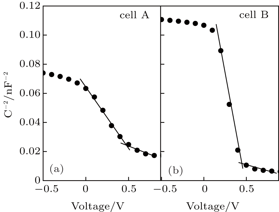
Figure 5 shows the relationship of the capacitances with bias voltage V. By the C– V test, one can obtain the information about the defect density on the p/i interface. It is shown that two linear changes for C− 2 with increasing V appear in the region from 0 V to 0.5 V and the region beyond 0.5 V, indicating that there is the depletion region shrinkage with V increasing. The first region is used to calculate the defect density in depletion layer for bulk μ c-Si:H, and the second region is used to obtain the sum of the defect density in the depletion layer of the bulk and that at the p/i interface. They are denoted as Ni and  , respectively. The density of states N can be calculated from the following equation:

and the depletion layer width Wd is calculated from the following equation:

where S is the cell area, ε 0 is the permittivity of vacuum, and ε r is the dielectric constant of μ c-Si:H (11.7 in this study).
The depletion layer width Wd is deduced from the capacitance at the point where the slope of the C− 2 plots starts to change. Thus the density of defect states at the i/p interface (Nif) can be estimated using the equation: 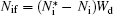 .[13, 14] The calculated values of Nif are 2.2 × 1012 cm− 2 and 5.0 × 1011 cm− 2 for cell A and cell B, respectively. The dramatic decrease of interface defect density clearly suggests that the p/i interface is well passivated.
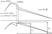
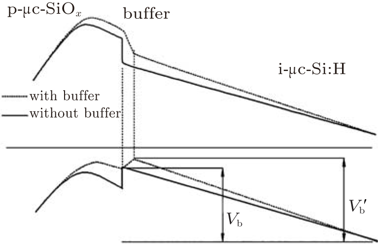
4. DiscussionTo reveal the reasons for increasing the photoelectric conversion of the cell B, the band diagrams of cells A and B are shown in Fig. 6. Firstly, the built-in voltage (Vbi) is generally viewed as the limit of the Voc. The Vbi can be analyzed according to the following equation:

where EFn and EFp are the Fermi levels of the n-layer and p-layer, Δ Ev and Δ Ec are the band offsets at the valence and conduction-band edges, respectively.[15] It is seen from Fig. 6 that the buffer layer provides a graded band gap at the interface between p- and i-layer and then reduces their band offsets, which obviously enhances the Vbi that contributes to the enhancement of the Voc. Compared with the fixed band gap buffer layers, the graded band buffer layer obviously smoothes the large potential drop at the p/i interface, which enhances the carrier transport and then improves the collection efficiency of carriers in i-layer. As a result, a higher EQE is observed through the spectrum region as shown in Fig. 3.
Secondly, the buffer layer reduces the generation of the incubation layer of the i-layer which further improves the carrier transport of i-layer near the interface.[16] By inserting the microcrystalline silicon oxide buffer layer, better ordered and more uniform microstructure of the i-layer can be achieved near the p/i interface. Meanwhile, the buffer layer will act as a barrier to suppress the boron diffusion since the i-layer of μ c-Si:H might slightly be of p-type due to a small amount of boron contamination.[17] Consequently, the density of deep level defects near the p/i interface is dramatically reduced by the decrease of the incubation layer and the suppression of the boron diffusion. The enhancement of EQE in short wavelength region reveals that the shrinkage of the interfacial defective region in the front part of i-layer. The calculated results from the C– V test show that the interface defect density of cell B decreases by one order of magnitude, which reduces the recombination rate of the p/i interface. The increase of n and the decrease of J0 also reflect that the recombination is suppressed.
5. ConclusionsThe effects of the graded band gap silicon oxide buffer layer inserted into the p/i interface on the μ c-Si:H cells are studied. The performance of cell B is improved after the inserting of the graded buffer layer. Band diagram analyses reveal that the inserted buffer layer smoothes the large potential drop at the p/i interface and then moderates the band gap mismatch, which enhances the carrier transport near the p/i interface. Better ordered and more uniform microstructure of the i-layer can be achieved near the p/i interface as a result of the reduction of the incubation layer after inserting the buffer layer. The buffer layer also acts as a barrier to suppress the boron diffusion. Since the high and uniform electric field is created by band-gap grading of the buffer layer, the carrier transport near the p/i interface is significantly enhanced and the density of defects near the p/i interface is dramatically reduced.


 , Yang Yan-Bin, Cong Ri-Dong, Chen Ying-Juan, Li Xiao-Wei‡