Characterizing silicon intercalated graphene grown epitaxially on Ir films by atomic force microscopy
[Zhang Yonga) , Wang Ye-Liang†a), b)  , Que Yan-De
a) , Gao Hong-Juna), b) ]
, Que Yan-De|
|


†Corresponding author. E-mail: ylwang@iphy.ac.cn
*Project supported by the National Basic Research Program of China (Grant Nos. 2013CBA01600 and 2011CB932700), the National Natural Science Foundation of China (Grant Nos. 61222112, 61390501 and 51325204), and Chinese Academy of Sciences (Grant Nos. 1731300500015 and XDB07030100).
An efficient method based on atomic force microscopy (AFM) has been developed to characterize silicon intercalated graphene grown on single crystalline Ir(111) thin films. By combining analyses of the phase image, force curves, and friction–force mapping, acquired by AFM, the locations and coverages of graphene and silicon oxide can be well distinguished. We can also demonstrate that silicon atoms have been successfully intercalated between graphene and the substrate. Our method gives an efficient and simple way to characterize graphene samples with interacted atoms and is very helpful for future applications of graphene-based devices in the modern microelectronic industry, where AFM is already widely used.
Graphene, a monolayer of carbon atoms arranged in a hexagonal lattice with relativistic electronic structure, [1] shows excellent electronic transport properties, [2] high thermal conductivity, [3] extraordinary elasticity and stiffness, [4] and a high on-off ratio in certain conditions, [5, 6] making graphene a promising candidate for new generation electronic devices.[7– 9] Till now, it has been challenging to prepare large-scale single crystalline graphene on semiconductors or insulators for direct applications. Among the developed growth methods of graphene, epitaxial growth of graphene on a transition metal substrate, acting as both template and catalyst, has been proven to be an effective way to grow high-quality, large-scale single crystalline graphene.[10– 15] However, the metallic substrate makes direct fabrication of graphene electronic devices difficult. Aiming to overcome this problem, silicon-layer intercalation between graphene and the metal substrate has been successfully developed.[16, 17] In such a structure, the intercalated silicon serves as a buffer layer that isolates graphene electronically from the metal substrate. Such a transfer-free method for growing high quality graphene opens the door to promising electronic applications. However, an effective and convenient way to identify graphene at mesoscopic scale after silicon intercalation is still highly anticipated.
In this work, we have epitaxially grown graphene on single crystalline Ir(111) thin films and successfully intercalated silicon atoms between graphene and the substrate. Such silicon-intercalated graphene samples have been characterized by atomic force microscopy (AFM), including phase image, force curves, and friction– force mapping. Based on the local and global information measured by AFM, we developed an efficient and simple way to characterize both graphene and silicon on the metal substrate, which is very useful for graphene-based device fabrication in the modern microelectronic industry, where AFM is already widely used.
The silicon interacted graphene samples are prepared by molecular beam epitaxy (MBE) under ultra-high vacuum condition (base pressure of 3 × 10− 10 mbar).[18, 19] The procedure for silicon layer intercalation is as follows: (I) epitaxial growth of monolayer single crystal graphene or isolated graphene islands on single crystalline Ir(111) film on Si(111) substrates with an yttria-stabilized zirconia (YSZ) buffer layer; [20] (II) exposing the graphene sample to silicon atoms evaporated by electron beam and then annealing it at 800 K to form an intercalated silicon layer between the graphene and the Ir(111) film.[16, 17] The AFM measurements were performed with a digital instrument, the Nanoscope IIIa, under ambient conditions using silicon cantilevers. The AFM tip we used is an NT-MDT high accuracy ETALON with a nominal spring constant of 4 N/m, which is 5.1 N/m after calibration by the Sader method.
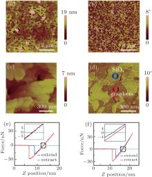
The samples used in our AFM measurements are graphene islands grown on the substrates. Figure 1(a) shows a representative topographic image of the silicon intercalated graphene on Ir(111) film, obtained by AFM in the tapping mode. The surface of the Ir film is dominated by large terraces with a roughness of < 1 nm. Structural defects-like grooves are visible between terraces.[18] The corresponding phase image of this topographic image is shown in Fig. 1(b). We can see that the surface is dominated by two kinds of regions contrasted clearly and colored by yellow and brown, respectively. We note that the silicon on the ‘ naked’ area (no graphene) is oxidized to silicon oxide (SiOx) after exposing in air. Thus two contrasted regions should be assigned to the graphene and SiOx.
 | Fig. 1. AFM characterization of Si intercalated graphene. (a) Representative topographic image of the Si intercalated graphene on Ir thin film. (b) The corresponding phase image with two distinct types of color contrasts (yellow and brown), indicating the locations of silicon oxide and graphene, respectively. (c) A zoomed-in image of panel (a). (d) The corresponding phase image of panel (c). All the above four images were acquired by tapping mode with a scanning rate of 1 Hz. (e) and (f) Force curves acquired at the locations marked by red and blue circles in panel(d), respectively. The red and blue curves correspond to retracting and extending modes, respectively. The cross points of the green dashed-line and the force curves indicate that the tip reaches a balance status of repulsive and attractive forces. The insets are the zoomed-in force curves from the black dashed squares shown in panels (e) and (f). |
In order to distinguish the locations of the graphene and SiOx, we further compared the topography and phase information of our samples. A zoomed-in topographic image and its corresponding phase image are shown in Figs. 1(c) and 1(d), respectively. From the topographic image, one can only obtain the height information of the samples. In Fig. 1(c), we can only see a clear height difference between the terraces from the substrate; however, such difference is not clear within each terrace, suggesting that it is difficult to distinguish graphene and SiOx from the topographic image. However, from the corresponding phase image [Fig. 1(d)], we can clearly see two types of regions contrasted differently, regardless of the height changes between terraces in the sample [Fig. 1(c)]. Such a phase difference has been reported in the previous studies, demonstrating that the phase signal of the AFM is sensitive to the composition of materials due to the differences in local energy dissipation.[21– 23] In our case, we can use the phase information (showing the two different types of regions) to determine the boundaries between graphene islands and SiOx, however, it is still impossible to ascribe the exact locations for both graphene and SiOx.
In order to determine the correspondence between the types of regions in the phase image and the types of materials, we further tested the samples by force curve measurements. The force curve has been widely used to probe the interaction between the AFM tip and the surface by recording the cantilever deflection as a function of the approach-retraction travel distance. Figures 1(e) and 1(f) show the force curves measured at the yellow and brown regions, respectively. In these force curves, the force is always zero before the AFM tip touches or after it detaches from the sample surface. While the tip touches the sample and the cantilever is parallel to the surface, the tip reaches a state wherein the Coulomb repulsive force and the van der Waals attractive force are balanced; thus the total force on the cantilever is relaxed to zero again [at about 15 nm in Fig. 1(e) and about 22 nm in Fig. 1(f)]. At this zero force point, the retracting force curve (red) coincides well with the extending one (blue) at the brown region, as shown in the inset of Fig. 1(e), indicating no clear mechanical deformation in this region. However, in the yellow region, a clear displacement is observed between the retracting and extending force curves [indicated in the inset of Fig. 1(f)]. Such separation between retracting and extending curves suggests a mechanical deformation occurred in the yellow region during the AFM force curve measurement.
It is known that mechanical deformation of silicon oxide can be induced by nanoindentation, [24, 25] while graphene has been proven to be the strongest material and, hence, is not easily deformed.[4] So we can attribute the yellow region, where a clear mechanical deformation is revealed in the force curve, to the SiOx. The brown region (without mechanical deformation) can be attributed to graphene. Thus, we identify graphene and SiOx by combining analysis of the force curves and the color contrast in the phase image. Furthermore, by calculating the area of the dimmer regions, we can get a coverage of 51.5% for graphene in the sample presented in Fig. 1(d).
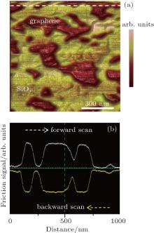
The silicon intercalated graphene can be further characterized by friction force microscopy (FFM).[26, 27] FFM is derived from the AFM contact mode and it is mapped by the torsion of the cantilever. Figure 2(a) shows a typical friction force map of the sample. The typical trace (in white) and retrace (in yellow) profiles taken along the blue dotted line (in Fig. 2(a)) are shown in Fig. 2(b). In these profiles two stages with an obvious difference in the values of friction force (as shown by valleys and peaks) are clearly visible, corresponding to two regions identified by different colors in Fig. 2(a), where a brighter color represents a higher friction force. The bright region can be easily assigned to the SiOx because it has a higher friction coefficient than that of graphene.[28– 30] Then the dimmer region is graphene, which has a lower friction coefficient.
 | Fig. 2. Friction force microscopy (FFM) characterization of Si intercalated graphene on Ir thin film. (a) Friction-force mapping with a forward scanning direction of the sample. The lower friction region (in brown) is assigned to graphene and the higher friction region (in yellow) is SiOx. This image was acquired in contact mode with a scanning rate of 1 Hz. (b) The corresponding friction signals of the trace and retrace processes taken along the white dashed line in panel (a). |
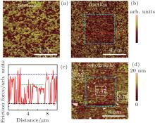
Interestingly, we find that the contrast of the friction– force mapping can be changed by repeated scanning at the same location of the sample, suggesting a change of the friction– force of the sample surface. Figure 3(a) is a friction– force mapping of silicon intercalated graphene on Ir film in a range of 5 μ m× 5 μ m. We then performed the second scan in a larger range of 10 μ m× 10 μ m centered at the same location as that of Fig. 3(a). The corresponding friction– force mapping is shown in Fig. 3(b). We find the location scanned twice (with the same size of Fig. 3(a)), marked by a blue dotted-square in the center of Fig. 3(b), becomes dimmer than the surrounding region where only one scan is performed. We note that no distinct height change has been found in the corresponding topographic image [Fig. 3(d)]. Such a dim area in the friction– force mapping suggests a lower friction, revealing a decreasing of the friction force in this area after a repeated scanning. Figure 3(c) is the friction– force profile extracted along the white dotted line of the friction– force mapping in Fig. 3(b). We can find three typical values of the friction force, as marked by three dashed lines with different colors. The largest friction force (near the purple dashed-line), can be ascribed to the SiOx, whereas the lowest friction force (near the black dashed-line) belongs to graphene due to its low friction coefficient. Besides these two values, an intermediate value of the friction force is also observed (near the green dashed-line) in the middle square region of Fig. 3(b), where the surface has been scanned twice, suggesting a decrease of the friction force coefficient of SiOx after increasing the AFM scanning times.
 | Fig. 3. The effect of repeated scanning by AFM tip in contact mode. (a) Friction force map of the sample after the first scan. (b) The friction map obtained from a larger area centered in panel (a). The blue dotted-square indicates the region in panel (a) scanned repeatedly, where an obvious contrast difference can be observed, indicating that the friction coefficient is reduced by increasing the scan times. (c) Friction force profile taken along the red dotted-line in panel (b). Three horizontal lines across the profile were drawn to assess the change of the friction force. The friction in the middle part (indicated by the green dashed-line), the repeatedly scanned area, become smaller than those of the outside area (indicated by the purple dashed-line). (d) The corresponding topographic image of panel (b). The apparent roughness in the middle region (1.47 nm) marked by a white square is smaller than in the other two square regions (3.55 nm and 2.70 nm) outside. All measurements were made under contact mode with a scanning rate of 1 Hz. |
We further measured the roughness of three typical regions marked by white squares in Fig. 3(d). The AFM tip we used has a spring constant of 5.1 N/m, which is relatively stiff for the contact mode and may change the morphology and structure of the sample. The measured roughnesses of squares from upper-left to lower-right are 3.55 nm, 1.47 nm, and 2.70 nm, respectively. Obviously, the lowest roughness is from the center square which has been scanned twice, demonstrating a reducing of the roughness by repeating the scan. From the friction– force profile shown in Fig. 3(c), we know that the friction– force of the SiOx has been reduced in the central region, whereas the friction– force remains the same for graphene. Similar results with an unchanged friction force of clean graphene after repeated AFM scanning have been reported recently.[31] We can infer that the flattened surface (with) in the scanned area is mainly from a decreased roughness of the SiOx surface.
In Fig. 1(c), we can distinguish the distributions of graphene and silicon oxide in the phase image. We also find that there is no obvious height difference between these two regions on the same terrace in the topographic image in Fig. 1(d). We know that the thickness of mono layer SiOx is normally larger than that of single layer graphene. Such a similar height of graphene and SiOx suggests the existence of a silicon layer beneath the graphene layer because the total thickness of single layer graphene and the intercalated silicon layer is comparable to that of SiOx. Otherwise, a clear height difference should be observed between graphene and SiOx. Furthermore, the phenomenon that graphene’ s friction coefficient does not change after repeated scanning also proves that SiOx generally does not exist on the surface of graphene, otherwise the SiOx would be driven away by the repeated scanning and the friction force of the graphene region would also decrease.
A technique based on AFM to characterize silicon intercalated graphene on single crystalline Ir films is reported. By analysis of both the phase image and force curves, we can identify distributions of graphene and silicon oxide at the mesoscopic scale and extract the coverage of graphene. The friction– force mapping was also employed to make a distinction between graphene and silicon oxide, based on the difference in their friction coefficients. We also find that repeated scanning on the sample can dramatically reduce the roughness of the SiOx region, as proven by the friction– force mapping. We also confirmed the existence of the silicon layer beneath the graphene. Our method provides a convenient way to characterize graphene samples with intercalated atoms, and it would be appropriate for studying graphene on other substrates.
| 1 |
|
| 2 |
|
| 3 |
|
| 4 |
|
| 5 |
|
| 6 |
|
| 7 |
|
| 8 |
|
| 9 |
|
| 10 |
|
| 11 |
|
| 12 |
|
| 13 |
|
| 14 |
|
| 15 |
|
| 16 |
|
| 17 |
|
| 18 |
|
| 19 |
|
| 20 |
|
| 21 |
|
| 22 |
|
| 23 |
|
| 24 |
|
| 25 |
|
| 26 |
|
| 27 |
|
| 28 |
|
| 29 |
|
| 30 |
|
| 31 |
|