


Enhanced ultraviolet photoresponse based on ZnO nanocrystals/Pt bilayer nanostructure*
[Tong Xiao-Lina), b) , Xia Xiao-Zhib) , Li Qing-Xiaa)†  ]
]
]
|
|


†Corresponding author. E-mail: qingxia_li@hust.edu.cn
*Project supported by the National Natural Science Foundation of China (Grant No. 41176156).
The development of solution strategies for Zinc oxide (ZnO) quantum dots provides a pathway to utilizing ZnO nanocrystal thin films in optoelectronic devices. In this work, quasi-spherical ZnO quantum dots with a diameter of 5 nm are synthesized by using ethanol as a solvent. ZnO nanocrystal thin film is obtained by spin-coating ZnO quantum dots on a Au interdigital electrode (IDE)/Al2O3 substrate and annealing at different temperatures in order to yield the optimal photosensitive on/off ratio of ZnO. For further enhancing the responsivity, ion sputtering is utilized to deposit Pt nanoparticles on the surface of ZnO nanocrystal thin film, the responsivity of the ZnO/Pt bilayer nanostructure increases from 0.07 A/W to 54 A/W, showing that the metal/inorganic nanocrystal bilayer nanostructure can be used to improve the performance of optoelectronic devices. The excellent properties of ZnO/Pt bilayer nanostructure have important applications in future electronic and optoelectronic devices.
In the past few years, ZnO has becomes a promising material for applications in electronics, [1– 3] photonics, [4– 6] and sensing devices.[7– 9] It is very attractive in UV detection due to the large bulk band gap (3.37 eV) and exciton binding energy (60 meV at 300 K).[10– 12] By now, the effects of crystallographic orientation, oxygen partial pressure, post annealing treatments in H2 or O2 ambient, etc. on the photoconductivity relaxation have been widely investigated.[13– 16] With the increasing demand for UV detection, it is very important to fabricate ZnO-based UV photodetector with high performance. Some efforts have been made to obtain ZnO films with fast, sensitive, and high UV response either by modifying the nanostructure[17, 18] or appropriately doping[19, 20] or passivating the surface of ZnO.[21– 23]
As is well known, chemiabsorption sites and oxygen vacancies are the main factors regulating the photosensitivity of the ZnO film.[24– 28] The influences of microstructure and crystallographic orientation on the chemiabsorption sites and oxygen vacancies have been investigated in Refs. [29] and [30]. Zhang[16] and Sharma et al.[14] investigated the effect of crystallographic orientation on the photoresponse transient of ZnO thin film. The surface states passivation by an overlayer of N-doped ZnO or SiO2 on ZnO thin film was studied by Mollow.[31] Liu and Kim[24] used oxygen plasma to suppress the chemisorption effect and the oxygen vacancy of ZnO film. Besides these, the effect of ultrathin metal film on the photoresponse characteristic of the metal/ZnO bilayer structure has been studied.[32] In another study, Yadav et al.[33] investigated the effect of induced charges on the dynamics of photoconductivity relaxation of metal/ZnO. However, the above method is so expensive that it is hard to realize large area fabrication.
In the present study, ZnO quantum dot solution is spin-coating on Au interdigital electrodes/Al2O3 substrate using the layer-by-layer technique. The as-deposited thin films are annealed at different temperatures to improve the Ohmic contact characteristic of ZnO/Au IDE and yield smooth ZnO nanocrystal thin film.[34] The optimal on/off ratio of ZnO thin film is obtained when the anneal temperature is 600 ° C. The resistance of the Au electrode would decrease during the high temperature anneal.[35] However, the effect of the resistance change of the Au electrode on the photoresponse performance is negligible because the resistance of ZnO nanocrystal thin film is larger than that of the Au electrode. In order to study the effect of the surface state on the photoresponse performance of ZnO nanocrystal thin film and explore a novel method to enhance the responsivity, the optimal thin film was measured in air and a vacuum for revealing the importance of the surface state to the photoconductive performance of ZnO. Based on the results, a novel approach is explored by using plasma to passivate the surface state, and at the same time Pt nanoparticle was deposited onto ZnO nanocrystal thin film to form a ZnO/Pt bilayer nanostructure for the responsivity enhancement. The Pt nanoprticle is a gorgeous light trapping material due to the surface plasmonic effect.[36] It is able to increase the photocurrent under the condition of maintaining the thickness of the film. The antioxidant ability makes Pt more stable in air than Al and Ag, and Liu et al. reported that the dark current of ZnO/Pt is 3.5 times smaller than that of ZnO/Au while the responsivity was approximately equal. So a Pt nanoparticle is close to that in our experiment.[37] The UV responsivity of ZnO nanocrystal thin film increases from 0.07 A/W to 54 A/W. The results show that the photoresponse of ZnO nanocrystal thin film can be enhanced by using plasma treatment and Pt nanoparticles as a conductive island.
ZnO quantum dots (QDs) were synthesized by using the recipe of Spanhel and Anderson.[38] Zinc acetate (Zn(CH3COO)2· 2H2O), lithium hydroxide monohydrate (LiOH· H2O), absolute ethanol were used as starting materials. In a typical procedure, 1.10-g (5 mmol) zinc acetate was dissolved in 50-mL absolute ethanol under magnetic stirring at atmospheric pressure. Then 0.29-g (7 mmol) LiOH· H2O was dissolved in 50-mL absolute ethanol in an ultrasonic bath. The hydroxide-containing solution was added dropwise to the Zn(Ac)2 suspension under vigorous stirring at 0 ° C for 1 h. The reaction mixture became transparent when about 0.1 g of LiOH had been added. The ZnO quantum dots were retrieved by adding hexane/heptane to the final solution and followed by centrifugation and dispersed in ethanol. The whole process was repeated three times to remove the excess precursor. The final product was dissolved in chloroform and filtered to form 50 mg/mL. In order to avoid aggregation, a small amount of butylamine was introduced to make the solution stable.
Figure 1 shows the structure of the ZnO/IDE/Al2O3 photodetector. The spacing gap of Au interdigital electrodes was 300 μ m, and the lengths of the electrodes were all 3 mm. IDE/Al2O3 substrates were cleaned prior to film deposition in a sequence of 5-min sonification in ethanol, 5-min sonification in acerton, 5-min sonification in ethanol, 5-min sonification in deionized water to remove any bubbles, and finally dried by N2 flow.
 | Fig. 1. Schematic diagram of ZnO metal– semiconductor– metal (MSM) photoconductive photodetector. |
ZnO quantum dots thin film was fabricated in ambient air using layer-by-layer deposition technology. The spin-coating speed and the spin time were 1500 rpm and 30 s, respectively. The film was dried at 200 ° C for 10 min, and the process was repeated 3– 4 times to obtain smooth ZnO nanocrystals thin film. Finally, the films were annealed at 400 ° C, 500 ° C, 600 ° C, and 700 ° C for 2 h in a muffle furnace respectively, and denoted as S1, S2, S3, and S4 for convenience. The Pt nanoparticles were deposited onto ZnO nanocrystal thin film by utilizing ion sputtering, the vacuum degree was 0.1 Pa and the deposition times were 5 min, 10 min, and 20 min, respectively.
The morphologies and sizes of as-synthesized ZnO quantum dots were characterized by transmission electron microscopy (Tecnai G2 20 U-Twin). The absorption spectrum was measured by using a Perkin Elmer Lambda 35. The crystal structure and the surface morphology were characterized by x-ray diffraction (XRD, XRD-7000S/L) and atomic force microscopy (AFM, SPA-300HV), respectively. Photoelectric properties were measured by HP (HP 4140B) inside an optically and electrically sealed box. Lighting was generated through a functional generator (Agilent 33210A) controlled 370-nm light-emitting diode.
Figure 2 shows the XRD pattern and absorption spectrum and corresponding TEM image of as-synthesized ZnO quantum dots.
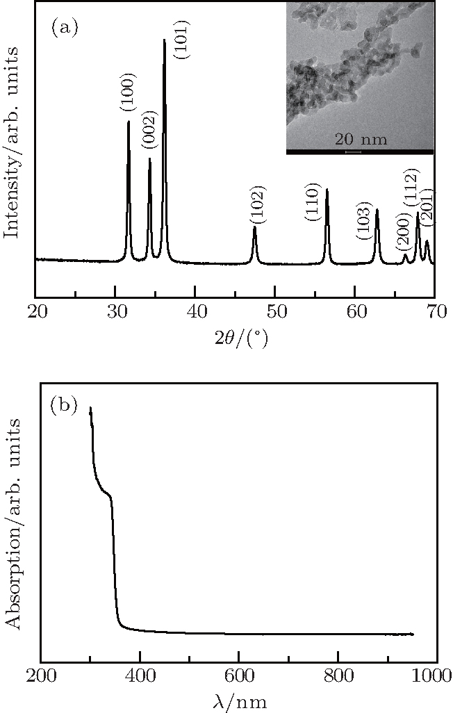 | Fig. 2. (a) XRD pattern and (b) absorption spectrum of as-synthesized ZnO quantum dots. Inset shows the corresponding TEM image of as-synthesized ZnO quantum dots. |
Based on the XRD pattern, the average size of ZnO quantum dot is estimated as 5 nm by using the Scherrer equation, [39] which accords well with the TEM observtion in the inset of Fig. 2(a), and all the diffraction peaks match well to hexagonal ZnO (JCPDS: 36-1451), indicating that the ZnO quantum dots have good crystallinity. Figure 2(b) shows the absorption spectrum of ZnO quantum dot, the absorption curve exhibits an intensive absorption in the ultraviolet region, owing to the large exciton binding energy of 60 meV.
The XRD patterns of the annealed specimens are shown in Fig. 3, the major diffraction peaks of the annealed ZnO thin films are also indexed. The results show that the width and intensity vary with annealing temperature. The grain sizes of the samples are estimated by using the Scherrer equation, and the grain sizes of four samples are about 20 nm, 26 nm, 30 nm, and 32 nm, respectively. The calculated results show that the grain size increases with the increasing of annealed temperature.
 | Fig. 3. XRD patterns of ZnO thin films annealed at different temperatures. |
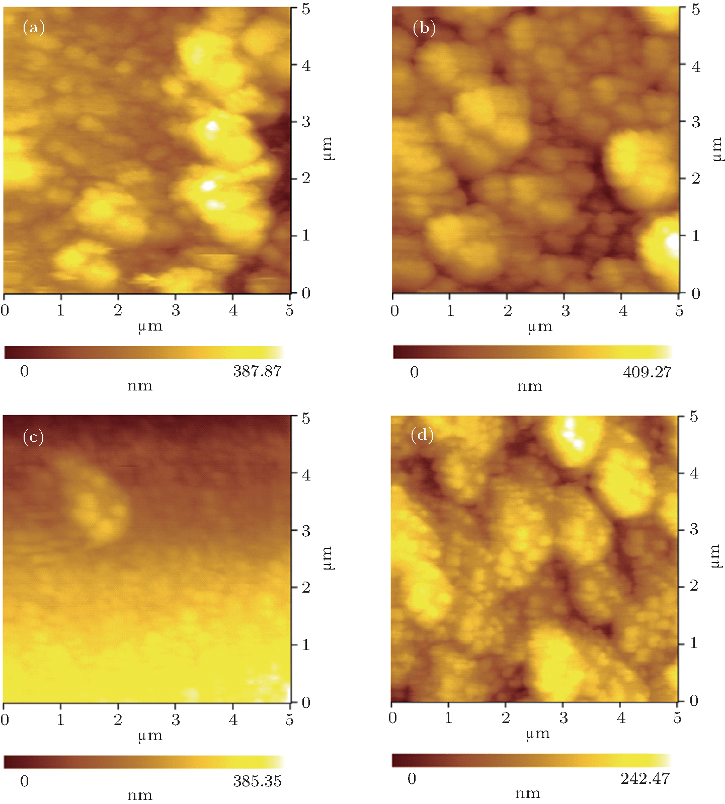 | Fig. 4. AFM images of ZnO thin films annealed at (a) 400 ° C, (b) 500 ° C, (c) 600 ° C, and (d) 700 ° C. |
Figure 4 shows the surface morphologies of the specimens. As shown in the figure, the surface morphology obviously varies with annealing temperature. The average grain sizes are uniform and the surface morphology is smooth when the annealing temperature is 600 ° C. However, the nanocrystals grow further and form clusters when the temperature increases to 700 ° C. The results indicate that the crystallinity is influenced by annealing temperature. ZnO grain formed at the low temperature has poor crystallinity, so does the crystallographic orientation, which are shown in Figs. 4(a)– 4(d). Although the crystallinity is important to semiconductor film, the annealing temperature could not be too high, because cracks and defects are formed at a high annealing temperature, and thus affect the responsivity of the ZnO nanocrystal thin film.
For studying the effect of annealing temperature on the photosensivity performance and obtaining the optimal samples, an HP 4140B is used to measure the photosensivity performance of the sample. Testing was done inside an optically and electrically sealed box. The results of dark current show that each of all ZnO films have an Ohmic contact with the Au electrode as illustrated in Fig. 5(a). The resistance of the film increases with annealing temperature rising. Of all the samples, sample S2 has the biggest dark current.
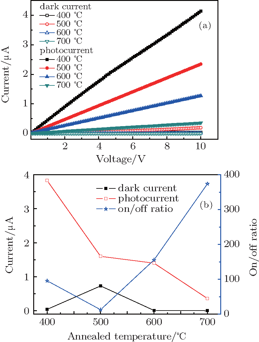 | Fig. 5. (a) I– V characteristics of ZnO thin films annealed at different temperatures. (b) Temperature-dependent UV sensitivity, dark current and photocurrent of ZnO thin film under a bias voltage of 10 V. |
As is well known, the conductivity is influenced by the crystallographic orientation of ZnO film. The results certify that the crystallinity of the S2 was worse than others, which is well consistent with the results from the XRD patterns and AFM spectra. This is because oxygen vacancy is donor-doping in ZnO film.[40] The resistance of the film increases with the oxygen vacancy density decreasing, and its conductance is caused by the oxygen vacancy and interstitial zinc, so the more perfect the crystal lattice, the lower the conductivity is. The effects of annealed temperature on dark current, photocurrent, and sensitivity are illustrated in Fig. 5(b), and the sensitivity is the on/off ratio (OFR) of current, which is defined by the following equation:[41]

Consider the characteristics of XRD and AFM, then the optimized annealing temperature will be 600 ° C.
For investigating the photoconductive mechansim of ZnO, the S3 is placed into a sealed quartz tube and the vacuum degree could be controlled. Figure 6(a) shows representative device responses to 390-nm monochromatic illumination at an intensity of 0.26 mW/cm2 in a vacuum and air. It could be seen that the photoresponse of ZnO is primarily attributed to the oxygen chemisorption process at the surface of ZnO film. The photoconductivity mechanism of ZnO film in air is shown in Fig. 6(b). The absorbed oxygen forms a barrier at the surface of the ZnO, the transport of the carriers is disturbed by the barrier, so the dark current is low. Under the UV irradiation, the desorbed process releases the electrons and the photocurrent increases with the decrease of resistance. Compared with the photocurrent in the case of the vacuum in Fig. 6(a), the photocurrent in air is low. The results certify that the absorbed oxygen blocks the transport of the carriers in the ZnO thin film.
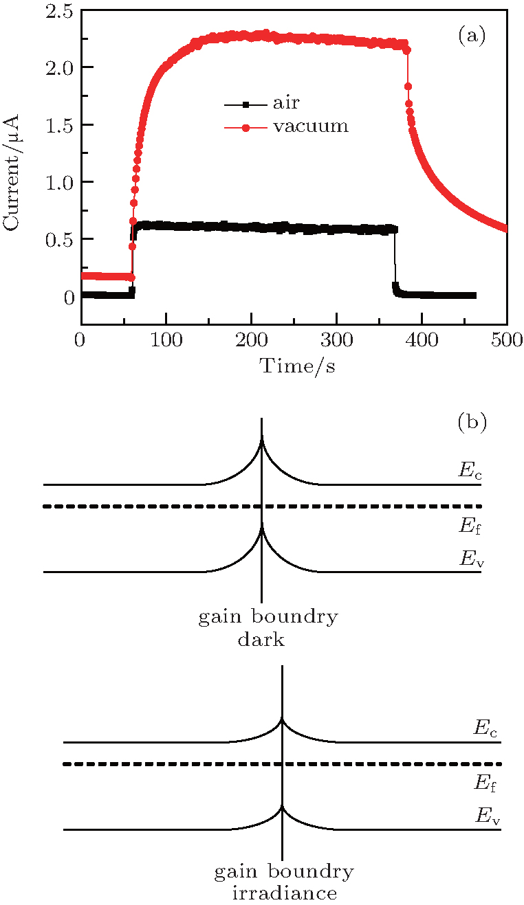 | Fig. 6. (a) On/off switching states of S3 device measured in air and a vacuum at an incident light density of 0.26 mW/cm− 2 and a bias voltage of 10 V, (b) band-edge diagrams of a single grain boundary of ZnO before and after UV, depicting the change in Shottky-barrier height. |
 | Fig. 7. On/off switching states of ZnO and ZnO/Pt devices at an incident light density of 0.26 mW/cm− 2 and a bias voltage of 10 V and (b) energy diagrams of ZnO with and without Pt nanoparticles. |
In order to reduce the surface state density and obtain an enhanced UV photodetector, sample S3 is covered with Pt nanoparticles by using ion sputtering. The advantages by using ion sputtering are that not only the low vacuum condition provided oxygen plasma which can passivate the surface state of ZnO film, but also the incorporated Pt nanoparticles provided a conductive tunnel for carrier transport. According to Liu et al.’ s study, [37] the results of spectral photoresponse showed that photoresponsivity enhancement of ZnO with metal (Au or Pt) relates to the plasmonic effect: these “ conductive islands” of Pt nanoparticles increase the “ effective mobility” and hence result in the increases of both dark current and photocurrent as shown in Fig. 7(a). The corresponding energy diagrams of ZnO[42] with and without Pt nanoparticles are shown in Fig. 7(b).
Testing is performed inside an optically and electrically sealed box, the lighting is produced by using 390-nm monochromatic illumination at an intensity of 0.26 mW/cm2. It is known that an important detectivity of photodetector is represented by the responsivity. The responsivity can be expressed as[43]

where Ip is the photocurrent and Popt is the power of incident light. The responsivity of the ZnO/Pt bilayer device increases from 0.07 A/W to 54 A/W, compared with that of the bare ZnO: the responsivity of ZnO/Pt is about three orders of magnitude higher. The rise time and decay time are defined as the times taken for the signal to increase from the dark current to 90% and drop off from maximum to 10%[44] respectively. It should be noticed that although the responsivity of ZnO/Pt is poorer than of other UV photodetectors, the photocurrent significantly increases by utilizing this simple method, and the results are summarized in Table 1. We believe that the performance of the photoconductor photodetector can be effectively improved by forming a semiconductor/metal bilayer nanostructure, with the spacing gap of the electrode, applied voltage, carrier mobility, and film thickness of the thin film kept unchanged.[43]
| Table 1. Comparison of performance between ZnO/Pt bilayer photodetector and other photodetectors. |
In this work, the enhanced photoresponse performance of ZnO nanocrystal thin film is obtained by forming ZnO/Pt bilayer nanostructure. The as-synthesized ZnO quantum dots are used to prepare thin films by spin-coating solution on Au IDE/Al2O3 substrates and annealing at different temperatures. The smooth ZnO nanocrystal thin film can be obtained when the annealing temperature is 600 ° C. Pt nanoparticles are further deposited onto ZnO nanocrystals thin film to form bilayer thin film. Owing to the improved carrier transport, the responsivity greatly increases from 0.07 A/W to 54 A/W. The excellent photoelectric properties of the ZnO/Pt bilayer nanostructure make this kind of material an important candidate for high-performance electronic and optoelectronic devices with enhanced properties.
| 1 |
|
| 2 |
|
| 3 |
|
| 4 |
|
| 5 |
|
| 6 |
|
| 7 |
|
| 8 |
|
| 9 |
|
| 10 |
|
| 11 |
|
| 12 |
|
| 13 |
|
| 14 |
|
| 15 |
|
| 16 |
|
| 17 |
|
| 18 |
|
| 19 |
|
| 20 |
|
| 21 |
|
| 22 |
|
| 23 |
|
| 24 |
|
| 25 |
|
| 26 |
|
| 27 |
|
| 28 |
|
| 29 |
|
| 30 |
|
| 31 |
|
| 32 |
|
| 33 |
|
| 34 |
|
| 35 |
|
| 36 |
|
| 37 |
|
| 38 |
|
| 39 |
|
| 40 |
|
| 41 |
|
| 42 |
|
| 43 |
|
| 44 |
|
| 45 |
|
| 46 |
|
| 47 |
|
| 48 |
|
| 49 |
|