


Progress in research of GaN-based LEDs fabricated on SiC substrate*
[Xu Hua-Yonga), b) , Chen Xiu-Fanga) , Peng Yana) , Xu Ming-Shenga), c) , Shen Yana), c) , Hu Xiao-Boa)†  , Xu Xian-Gang
a), c) ]
, Xu Xian-Gang|
|

 , Xu Xian-Gang
†Corresponding author. E-mail: xbhu@sdu.edu.cn
*Project supported by the National Basic Research Program of China (Grant No. 2011CB301904) and the National Natural Science Foundation of China (Grant Nos. 11134006 and 61327808).
The influence of buffer layer growth conditions on the crystal quality and residual stress of GaN film grown on silicon carbide substrate is investigated. It is found that the AlGaN nucleation layer with high growth temperature can efficiently decrease the dislocation density and stress of the GaN film compared with AlN buffer layer. To increase the light extraction efficiency of GaN-based LEDs on SiC substrate, flip-chip structure and thin film flip-chip structure were designed and optimized. The fabricated blue LED had a maximum wall-plug efficiency of 72% at 80 mA. At 350 mA, the output power, the Vf, the dominant wavelength, and the wall-plug efficiency of the blue LED were 644 mW, 2.95 V, 460 nm, and 63%, respectively.
Its small lattice mismatch and high thermal conductivity make silicon carbide (SiC) the ideal substrate for gallium nitride (GaN) growth.[1, 2] Though GaN-based LEDs on SiC substrate have been commercially available, [3, 4] further work should be done to reduce their cost and increase their brightness. The most effective way to reduce cost is to use larger SiC substrate, which is very challenging because the growth temperature of SiC crystal exceeds 2000 ° C and the heat and mass transfer during SiC sublimation growth in a graphite crucible is hard to control.[5] Besides, the quality of SiC also needs to be improved by eliminating micropipe defects, which extend into GaN epitaxial layers and deteriorate the LEDs’ performance. For GaN heteroepitaxial growth on SiC substrate, residual stress and strain are a crucial problem. Mostly AlN has been used as a buffer layer.[2] Though the quality of GaN film was improved by optimizing the AlN buffer layer growth conditions, large dislocation density and residual stresses still exist in the GaN epilayer. The refractive index of SiC is about 2.6. For GaN-based LED chips on SiC substrate, a significant amount of light emission from the active layer is trapped inside the semiconductor structure because of total internal reflection (TIR). The extraction efficiency could be improved using a shaped SiC substrate, [1, 2, 6] but improvement is relatively small when the chip size exceeds 1 mm × 1 mm.
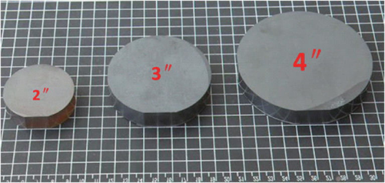
In the present work, four-inch (1 inch = 2.54 cm) diameter SiC substrates with low-density micropipes were prepared. An AlGaN buffer layer was grown to decrease the dislocation density and the residual stress of the GaN film. GaN-based LED chips on SiC substrate with flip-chip structure and thin film flip-chip structure were fabricated and investigated respectively.
SiC crystals were grown by the sublimation method with an inductively heated graphite crucible. Carbon-faces of 4H– SiC substrates were seeded to grow 4H– SiC boules. The growth temperature was in a range from 2200 ° C to 2300 ° C, which was measured by an optical pyrometer at the top of the crucible during growth. After growth, the crystals were sliced with a diamond wire saw perpendicular to the c-direction, and then were lapped and polished with diamond slurries step by step.
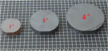
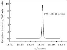
SiC is a polytypic material. Due to the low stacking fault energy, [7] it is difficult to restrict syntaxy (parasitic polytype formation) during the bulk crystal growth and to grow a single-polytype material. 6H and 15R-SiC are often parasitic with 4H– SiC applications in crystals grown via the sublimation method.[8] It is important to control the polytype for application in semiconductor devices because the band gap and electrical properties of SiC varies with polytype. The influences of growth parameters, such as growth temperature, [9, 10] supersaturation, [11, 12] vapor phase composition and system pressure, [12, 13] and face polarity of seed crystal[14] on the polytype stability have been discussed sufficiently. By identifying different polytypes in SiC at the same time by high resolution x-ray diffractometry (HRXRD) and Raman spectroscopy, we investigated the formation mechanism of SiC polytypes, and eventually pure 4H– SiC crystal without other polytypes was obtained. Since 2012, 3 inch– 4 inch (1 inch = 2.54 cm) 4H– SiC single crystals were grown with high structural quality, as shown in Fig. 1. The whole 3 inch– 4 inch wafers were scanned by Raman mapping mode with the step of 5 mm by 5 mm. The result showed that the proportion of 4H polytype was 100%. Figure 2 shows the 3-inch 4H– SiC Raman mapping image. HRXRD was used to characterize the structural quality of 4H– SiC crystal. The full width at half maximum (FWHM) for rocking curve of (0004) reflection is 12 arcsec, as shown in Fig. 3.
 | Fig. 1. The 2 inch– 4 inch inch 4H– SiC single crystals. |
 | Fig. 2. The 3-inch 4H– SiC Raman mapping image. |
 | Fig. 3. Rocking curve of (0004) reflection for 4H– SiC substrate with FWHM 21 arcsec. |
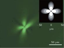
To meet the challenges of commercialization of SiC semiconductors, specific efforts have been made toward larger diameter and higher quality SiC bulk crystals. Great advances have been made in improving the quality of SiC crystals, especially in the reduction of micropipe defects. Generally, micropipes which lie along the c-axis in hexagonal or rhombohedral crystals, are often found in sublimation-grown SiC crystals. Any micropipe existing in the device area limits high voltage operation. Even one micropipe in the active area of a high voltage SiC device will lead to electric breakdown. Therefore, micropipes are the major obstacles to the production of high-performance SiC-based devices, especially at high voltages or for high current power devices.[15] Micropipes have been observed by atomic force microscopy, transmission electron microscopy, x-ray topography, and so on. There has been much debate about the nature of micropipes, and several models have been proposed to illuminate the formation mechanism of micropipes.[16– 18] Most views on micropipe formation in PVT-grown SiC crystal are based on Frank’ s theory[19] that a micropipe is a hollow-core screw dislocation with a huge Burgers vector (several times the c-lattice constant for 6H– SiC or 4H– SiC) and with the diameter of the core having a direct relationship to the magnitude of its Burgers vector.
Ning et al.[20] observed and simulated the birefringence images of micropipes in 6H– SiC crystals. Based on Frank’ s theory, the intensity contours of birefringence images for micropipes viewed end-on in SiC crystals has been derived by considering the photoelastic anisotropy of silicon carbide. The results are in good agreement with experimental observations. Figure 4 shows a microscopic image of a micropipe observed by a polarizing optical microscope and the corresponding simulation image.
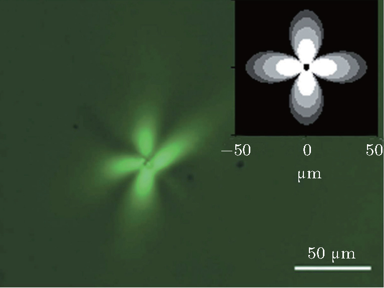 | Fig. 4. Birefringence image of a micropipe observed by a polarizing optical microscope and the corresponding simulation image shown in the inset at the upper right.[20] |
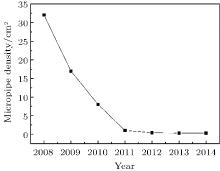
According to the above discussion, a series of measures were taken. A significant reduction in micropipe density was achieved. Figure 5 shows a tendency curve of the average micropipe density for a 3-inch 4H– SiC wafer displaying an improvement of crystal quality. It is observed that from 2008, the micropipe density has been reduced continually. Since 2012, the micropipe density has been less than 0.5/cm2 for 3-inch 4H– SiC substrates.
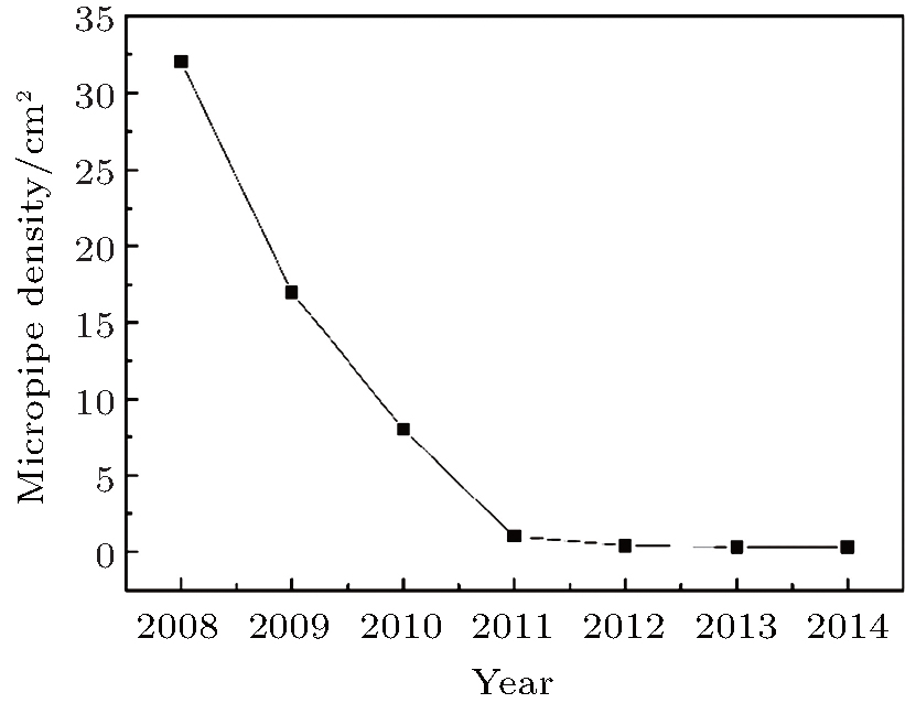 | Fig. 5. Reduction of average micropipe density for 3-inch 4H– SiC wafer. |
The transmissivity of SiC substrates, which is directly related to impurity concentration, greatly affects the LED luminescence efficiency. More interesting is the nature of different impurities, especially dopants like boron, aluminum or transition metals.[21] By optimizing technological conditions of the crystal growth and purifying source powder, SiC crystals exhibit strong improvement in purity. Secondary ion mass spectroscopy (SIMS) analysis has been performed to study the impurity concentration. The data are shown in Table 1.[22] This result shows that after performing the purification process, the impurity concentration value is reduced significantly. The transmissivity in the visible light range for high purity substrates rises greatly, by 10%– 20% compared with that for unpurified substrates. The rise of transmissivity favors the light extraction efficiency of GaN-based LED on SiC substrate.
| Table 1. SIMS analysis of high purity SiC substrates (in unit cm− 3), superscript a indicates the concentration lower than detection limit.[22] |
GaN films were grown on conventional and high purity c-plane 4H– SiC substrates by a VEECO K465 metal– organic chemical vapor deposition (MOCVD) system. Nitrogen and hydrogen were used together as the carrier gases. Ammonia, trimethyl gallium (TMG), and trimethyl aluminum (TMAl) were used as sources of N, Ga, and Al, respectively. The SiC substrates were pre-treated in hydrogen ambience at a temperature of 1080 ° C for 500 s in the MOCVD reactor. A buffer layer and a u-doped GaN layer was deposited subsequently. Three samples were prepared with different growth conditions of buffer layers. Sample A has an AlN buffer layer grown at 1020 ° C. Samples B and C have AlGaN buffer layers grown at 1020 ° C and 1100 ° C, respectively.[23] The Al content of AlGaN is 10%.
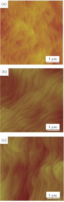
The surface morphologies of the three samples were characterized by atomic force microscopy (AFM), as shown in Fig. 6. Sample A has a much higher density of atomic steps and narrower terrace widths compared with samples B and C. Dislocations exist at the intersection of the atomic steps. It is obvious that the dislocation density in sample A is greater than that in sample B, and the dislocation density in sample C is the lowest.
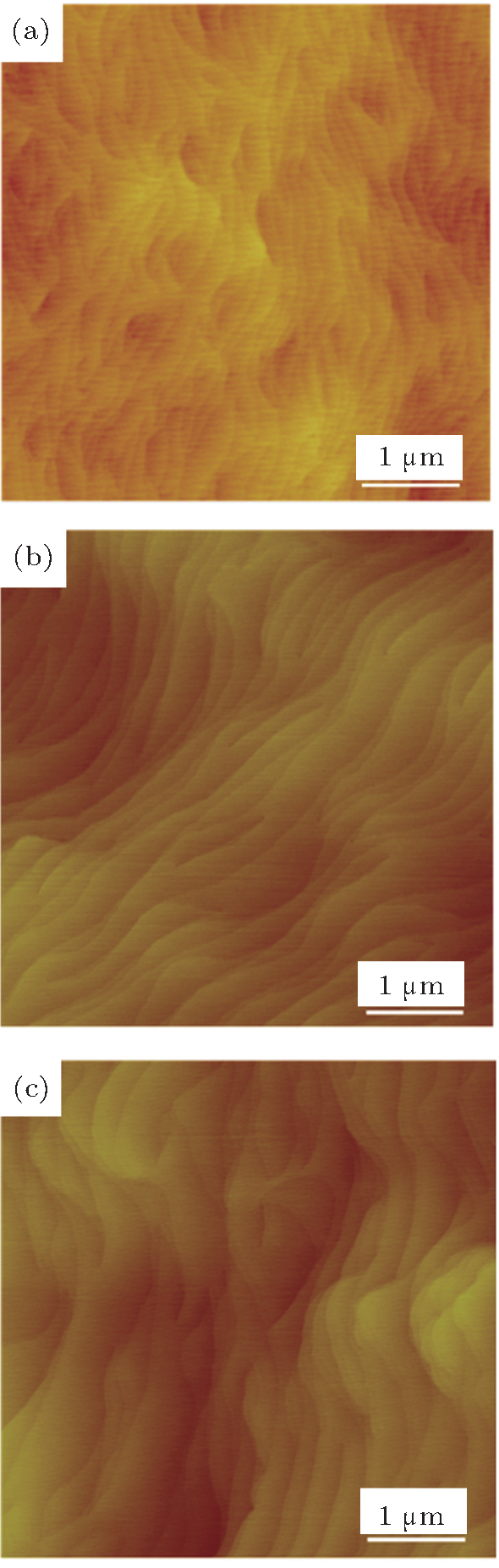 | Fig. 6. AFM images of GaN films grown on SiC substrates (a) sample A; (b) sample B; (c) sample C.[23] |
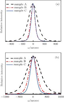
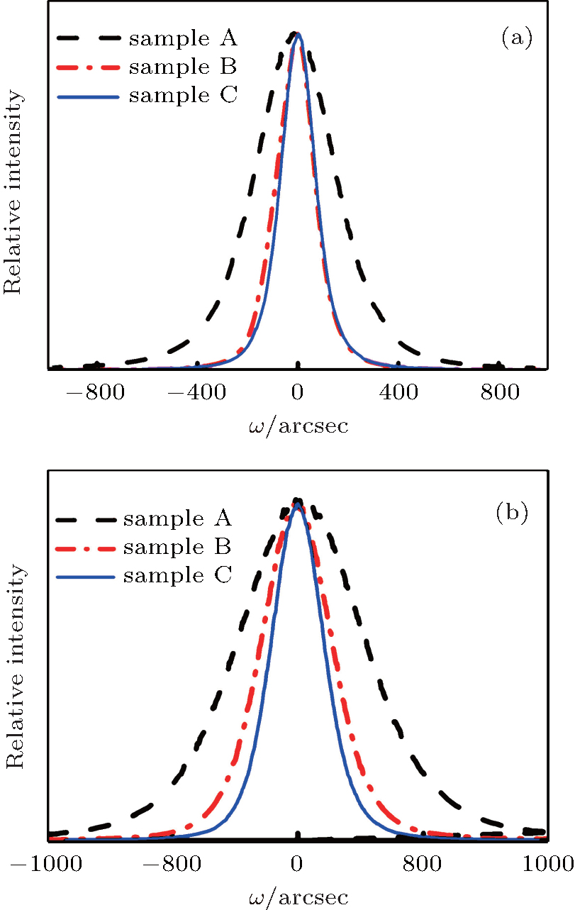
To confirm the above deduction, HRXRD was used to assess the structural quality of epitaxial layer. Figure 7 shows the HRXRD rocking curves of (0002) and (10-12) reflections of the GaN films respectively. Obviously, the FWHM of the rocking curves of the sample with AlN buffer layer is much wider than that of the samples with an AlGaN buffer layer. That means the AlGaN buffer layer improves the quality of GaN film grown on SiC substrate. When the growth temperature of the AlGaN buffer layer increases from 1020 ° C to 1100 ° C, the FWHM of (0002) reflection remains unchanged, but the FWHM of the (10-12) plane decreases. This indicates that a higher growth temperature of the AlGaN buffer will significantly reduce the edge dislocation density, but has no effect on screw dislocation density of GaN film. AlGaN buffer grown at higher temperature has a lower density and larger size nucleation islands, which is shown in Fig. 9. Edge dislocation usually exists at the grain boundary of adjacent islands. Such edge dislocation density of sample C is smaller than that in sample B. However, screw dislocations originate mostly from lattice mismatch. Increasing the growth temperature of AlGaN buffer has a small effect on the lattice mismatch. Thus the screw dislocation density of sample C remains unchanged. High temperature growth of AlGaN buffer could significantly improve the quality of GaN film on SiC substrate, and the FWHMs of (0002) and (10-12) reflections are reduced to 161 arcsec and 244 arcsec, respectively.
 | Fig. 7. High resolution XRD rocking curves of GaN films: (a) (0002) reflection; (b) (10-12) reflection.[23] |
Photoluminescence (PL) spectroscopy is another important method to study the GaN film. Besides near-band-edge photoluminescence emission of GaN, yellow-band luminescence (YL) bands were observed as shown in Fig. 8. The YL is a broad Gaussian-shaped emission centered at 2.2 eV– 2.3 eV, which is related to defects and/or impurities in GaN.[24] The YL intensity of sample C is weaker than those of samples A and B. It is consistent with AFM and HRXRD results.
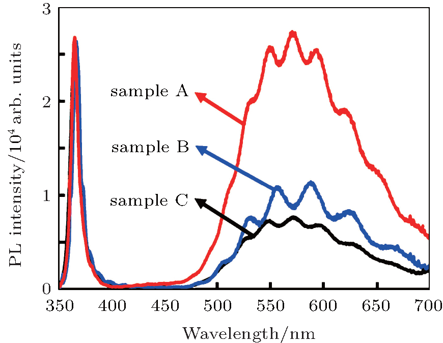 | Fig. 8. Room temperature photoluminescence spectra of three samples.[23] |
To further study the effects of buffer layer growth conditions on the quality of GaN film, a single buffer layer was prepared. An aluminum atom has low migration activity, which leads to a high nucleation density of AlN on an SiC substrate. The surface morphology of AlN buffer layer is shown in Fig. 9(a). A large number of AlN nucleation islands are visible. When GaN grows laterally on these islands, dislocations are generated at the boundaries of adjacent islands. Gallium atoms have higher migration activity than aluminum atoms. Thus the nucleation density of AlGaN decreases. Meanwhile, the size of AlGaN islands increases, as shown in Figs. 9(b) and 9(c). As the growth temperature of the AlGaN buffer was elevated from 1020 ° C to 1100 ° C, Al and Ga atoms get more thermal energy and higher mobility, and a better AlGaN buffer layer with lower density and larger nucleation islands is obtained, which benefits the subsequent GaN growth.
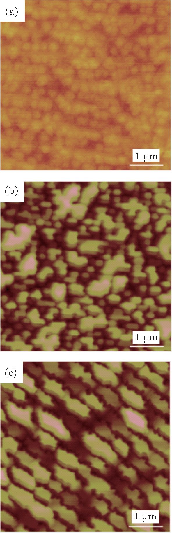 | Fig. 9. AFM images of different buffer layers. (a) AlN nucleation layer; (b) AlGaN nucleation layer grown at 1020 ° C; (c) AlGaN nucleation layer grown at 1100 ° C.[23] |
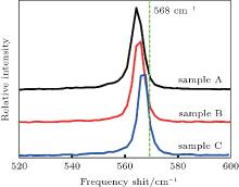
Stress is another technological issue for GaN growth on SiC substrate. The stress in GaN film is caused by the lattice and thermal mismatches between SiC and GaN. It impacts the curvature of the wafer and a temperature distribution on it, leading to inhomogeneities of the In-composition and emission wavelength. Once the stress exceeds the critical value, cracks of the GaN film will occur. Raman spectroscopy is used to measure the magnitude of stress in GaN film. GaN has a hexagonal structure belonging to the C6v symmetry group. Stress in GaN (0001) film is biaxial and causes a Raman shift of the E2 (high) mode. The Raman spectra are shown in Fig. 10. All three samples show blue Raman shifts compared with the theoretical value (568 cm− 1). This means that the GaN grown on SiC substrate has tensile stress. The shift of E2 (high) mode of GaN film grown on high temperature AlGaN buffer is minimal. The results indicate that an AlGaN buffer reduces stress in GaN, mostly because the thermal expansion coefficient of AlGaN is much smaller than that of GaN, which alleviates the thermal mismatch between SiC and GaN.
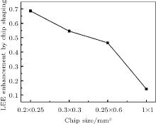
GaN and SiC are transparent substrate materials, which is conducive to the light extraction of GaN-based LEDs on SiC substrate. However, the refractive indexes of GaN and SiC are about 2.3 and 2.6, respectively. Most of the light emitting from the InGaN active layer is trapped inside the LED chip because of total internal reflection (TIR). Chip shaping technology is an effective way to improve the light extraction efficiency (LEE) of LEDs, such as red LED with transparent GaP substrate[25] and blue GaN LED with transparent SiC substrate.[3, 4] Further simulation work was carried out by Schad et al., and a sidewall angle of 64° was optimal for a truncated pyramid GaN-based LED on SiC substrate.[6] For the model, the bottom and top sizes are 200 μ m × 200 μ m and 300 μ m × 300 μ m, with a total thickness of 100 μ m. By means of simulation, we found that as the chip size increases the enhancement of LEE by chip shaping decreases dramatically. The relationship between the chip size and the enhancement of LEE is shown in Fig. 11. When the chip size reaches 1 mm × 1 mm, the enhancement is less than 15%. Baur et al. fabricated an LED array to get large-area chips.[26] The process is complicated and not suited for mass production.
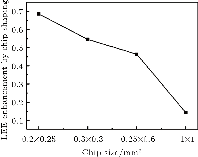 | Fig. 11. Relationship between the chip size and the enhancement of LEE for truncated pyramid GaN-based LED on SiC substrate |
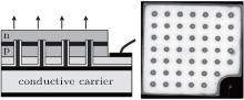
The flip-chip LED (FC-LED) technique is an effective way to enhance heat dissipation and the optical output of a high power LED. We grew InGaN/GaN LEDs on SiC substrates with different extinction coefficients and fabricated FC-LED chips with them.[27] The epitaxial structure our GaN on SiC LED included a 10-nm thick nucleation layer, a 3-μ m thick undoped GaN film, a 2-μ m thick n-type GaN layer with a doping concentration of 1 × 1019 cm− 3, twelve pairs of multiple quantum wells (MQW) with 3-nm thick wells and 10-nm thick barriers and a 300-nm thick p-type GaN layer with a doping concentration of 5 × 1019 cm− 3. To fabricate FC-GaN-on-SiC-LED (FC-SLED) chips, a standard photolithographic process was used to define the chips with a mesa size of 1 mm × 1 mm. Then, the wafer was partially dry-etched down to the n-type GaN by inductively coupled plasma (ICP) technology. A highly reflective silver film, which reflects light back into the substrate, was deposited as a p-type Ohmic contact metal on the surface of the wafer. A 1-μ m thick SiO2 layer was deposited as insulation for the p– n electrodes by plasma enhanced chemical vapor deposition (PECVD). A Cr/Au metal multi-layer was used as the n-type Ohmic contact layer and electrodes. A wedge blade was then used to bevel the substrate of the FC-SLEDs. Then the FC-SLED chips were bonded onto a silicon template with indium solder for optical and electrical measurements.
For FC-SLED, the oblique face of the beveled substrate can efficiently improve the LEE by reducing TIR. The obliquity angle α is defined as the angle between the sidewall and the horizontal plane of the beveled substrate, as shown in the inset of Fig. 12. The dependence of the LEE for the packaged FC-LED upon the obliquity angle α was simulated by using the ray tracing method. When the angle α is reduced to 40° , the LEE decreases slightly. The optimal obliquity angle for the best LEE in an FC-SLED is 60° . From the simulation results, the LEE of encapsulated FC-SLEDs on the 60° beveled substrate increases by 61% compared with that on the rectangular substrate (α = 90° ).
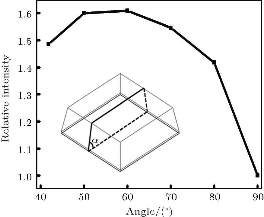 | Fig. 12. Simulated relative light output intensity of the FC-SLEDs as a function of oblique angle of SiC sidewall. Inset indicates oblique angle α .[27] |
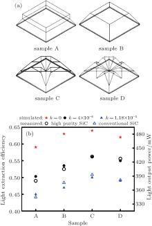
We designed four chips with different geometric shapes in order to further increase the LEE of the FC-SLEDs. At the same time, the influence of the absorption coefficient of the SiC substrate on LEE was studied. The simulation and experimental results are shown in Fig. 13. In the simulation, the extinction coefficient k was used to replace the absorption coefficient. The solid and hollow symbols correspond to the simulation and experimental results, respectively. Sample C has the best light output properties, in both simulations and experiments. The calculated LEE of FC-SLED with the “ X” pattern (sample C) reaches up to 64%, which is much greater than that of GaN LEDs with a pyramid reflector.[28] Sample D shows a smaller LEE than sample C, although it has a larger oblique face area (OFA). The reason is that sample D has a smaller top face area (TFA), which reduces the normal light extraction. The TFA and OFA should be balanced. The LEE of FC-SLEDs dramatically decreases as the extinction coefficient of the SiC substrate increases. The impurity in SiC plays an important role in absorption at the blue band. The extinction coefficient of high purity SiC is much smaller than that of conventional SiC; thus a high light output power is obtained for an LED on beveled high purity SiC substrate.
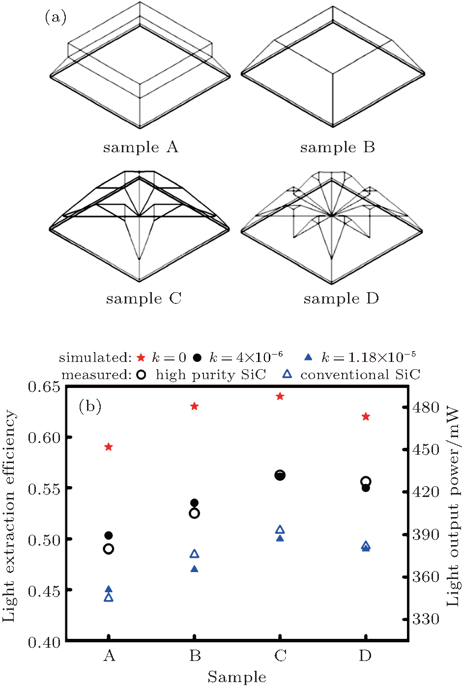 | Fig. 13. (a) Stereoscopic diagrams of FC-SLEDs with different substrate geometries; (b) LEEs and light output powers of samples A-D: red stars, black round dots, and blue solid triangles are simulated data; black hollow circles, and blue hollow triangles are experimental results.[27] |
Osram Opto Semiconductors GmbH developed “ UX:3” technology. The essential step in design and chip processing of UX:3 technology is the bonding of the epitaxial layer to a carrier wafer and subsequent removal of the growth substrate. The growth substrate of UX:3 InGaN chip is silicon. The UX:3 technology has a metal-free emissive side and a perfect lateral charge carrier spreading especially at high current, as shown in Fig. 14. The UX:3 chip shows about 30% more luminous flux than the conventional vertical thin-film chip.[29]
 | Fig. 14. Schematic cross section and luminance pattern at high current for UX:3 chip. |
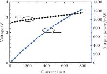
We developed similar chips on SiC substrate, calling them thin-film-flip-chip GaN-on-SiC LEDs (TFFC-SLEDs). The chip process of TFFC-SLEDs before wafer bonding is like that of FC-LEDs, including a reflective silver film on p-GaN, a 1-μ m thick SiO2 insulation layer, and a Cr/Au n-type Ohmic contact layer. The n electrode is set at the back of the alternative substrate by wafer bonding. The p electrode is placed on silver film after the growth substrate is removed, and partial GaN epi-layer is etched to expose silver film. The chip size is 1 mm × 1 mm. The difficulty to fabricate TFFC-SLEDs on SiC substrate is that SiC substrate is hard to remove since it has high hardness and is chemically inert. Conventional physical and chemical methods cannot remove the SiC substrate. We developed a way combining mechanical grinding and inductively coupled plasma (ICP) etching. The SiC substrate is thinned by mechanical grinding to a certain thickness and then etched by ICP. The ICP etching selection ratio of SiC and GaN is above 20, which prevents GaN film from over-etching. After the SiC substrate is removed, surface roughing is carried out on the n-face GaN with hot alkaline solution. The power– current– voltage (P– I– V) curves of TFFC-SLED with silicone packing are shown in Fig. 15. The output power of TFFC-SLED is 10% higher than FC-SLED. Because surface roughing of n-face GaN is more effective to improve LEE than flip-chip technology, similar technology has been applied to flip-chip LED on sapphire substrate.[30]
 | Fig. 15. The power– current– voltage (P– I– V) curves of the fabricated TFFC-SLED with silicone packing. |
Figure 16 shows the wall-plug efficiency (WPE) of the blue LED as a function of the injection current. The maximum WPE was 72% at 80 mA. At 350 mA, the output power, Vf, the dominant wavelength, and the wall-plug efficiency of the blue LED were 644 mW, 2.95 V, 460 nm, and 63% respectively. The Vf increased from 2.74 V to 2.95 V and the WPE decreased by 7.7% as the current increased from 80 mA to 350 mA. This means that the external quantum efficiency of the blue LED decreased only by 3.5% as the current increased from 80 mA to 350 mA. The excellent performance of the LED at high injection current is related to the high quality of the GaN film grown on SiC substrate and the high heat dissipation of the LED with thin film structure.
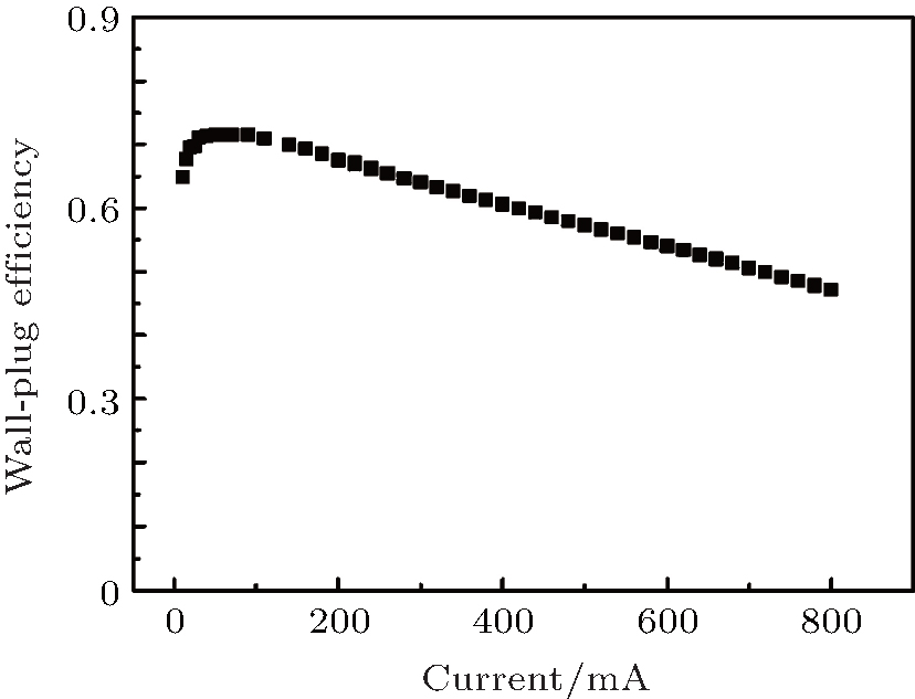 | Fig. 16. Wall-plug efficiency (WPE) of the blue LED as a function of the injection current. |
A review of research on GaN-on-SiC LED was provided. The diameter of SiC substrate was enlarged from 2 inches to 4 inches, which will reduce the cost of GaN-on-SiC LED significantly. Meanwhile, the quality of the SiC substrate was improved, e.g., the micropipe density was stabilized below 0.5/cm2, and high purity SiC substrate was obtained. GaN epitaxial layer was grown on AlGaN buffer instead of AlN to improve the structural quality of GaN. The AlGaN buffer exhibits superiority in the suppression of dislocation density and stress in GaN. To improve the LEE of GaN-on-SiC LEDs, we fabricated and studied two kinds of LED chips with flip-chip structure and thin-film-flip-chip structure, respectively. The LEE of FC-SLED was improved by optimizing geometric shapes and reducing the absorption coefficient of the SiC. TFFC-SLED shows a higher LEE, but the fabrication process is more complex, leading to relatively low yield and high cost. To make GaN-on-SiC LEDs more competitive in the application of solid-state lighting, further work should be done in technology for the growth of larger SiC substrates, technology for high-quality, low-stress GaN epitaxy, and technology for high-LEE, low-cost chips.
| 1 |
|
| 2 |
|
| 3 |
|
| 4 |
|
| 5 |
|
| 6 |
|
| 7 |
|
| 8 |
|
| 9 |
|
| 10 |
|
| 11 |
|
| 12 |
|
| 13 |
|
| 14 |
|
| 15 |
|
| 16 |
|
| 17 |
|
| 18 |
|
| 19 |
|
| 20 |
|
| 21 |
|
| 22 |
|
| 23 |
|
| 24 |
|
| 25 |
|
| 26 |
|
| 27 |
|
| 28 |
|
| 29 |
|
| 30 |
|