


Threshold switching uniformity in In2Se3 nanowire-based phase change memory*
[Chen Jiana), b) , Du Gangb) , Liu Xiao-Yanb)†  ]
]
]
|
|


†Corresponding author. E-mail: xyliu@ime.pku.edu.cn
*Project supported by the National Basic Research Program of China (Grant No. 2011CBA00604).
The uniformity of threshold voltage and threshold current in the In2Se3 nanowire-based phase change memory (PCM) devices is investigated. Based on the trap-limited transport model, amorphous layer thickness, trap density, and trap depth are considered to clarify their influences upon the threshold voltage and threshold current through simulations.
One of the most promising candidates of storage class memory (SCM)[1– 4] is the phase change memory (PCM) for its excellent endurance, long retention, faster write speed and scaling capability.[5– 8] PCM operates on the principle of threshold switching associated with the reversible phase change between the crystalline and amorphous states.[9, 10] The switching threshold voltage and current are not constant values and have a variation in different programming cycles. The uniformity of the threshold voltage and threshold current[11, 12] is extremely important for the PCM operation since they mark the boundary between the read and programming regime of the memory, especially for the future ultra-low voltage devices.[13, 14] Uniformity of threshold switching is both affected by device-to-device process induced variability and intra-device programming induced variability. Many studies have been done on the physics of threshold switching[15, 16] and the trap-limited transport model[22, 23] is currently widely used to explain most of the intra-device programming characteristics including threshold switching phenomenon. However, there have been a limited number of reports which provided clear explanations of the relationship between different localized states and the uniformity of threshold switching. In order to understand the physics behind the threshold switching uniformity, factors related to the localized states such as amorphous thickness, trap density, and trap depth should be investigated to explain the influences on the uniformity.
PCM in the form of nanowire[17– 20] allows the size of the centralized phase change region to be controlled, which offers a better method to investigate the threshold uniformity mechanism. Among the phase change materials, In2Se3 is more promising since it exhibits higher resistivity than GeTe or Ge2Sb2Te5 and its resistivity can be varied by a factor of 105 which enables the multilevel applications.[21] Besides, the programming power for the RESET operation of the nanowire-based In2Se3PCM is only tens of microwatts compared to the milliwatt power levels required by the conventional thin-film-based PCM.[18] In this paper, we focused on the intra-device threshold parameters characterization and analysis in nanowire-based In2Se3PCM. The experimental data were collected from the same nanowire device to avoid the device-to-device process induced variability on the threshold switching. First, the RESET operation was accomplished to get the amorphous state. Then we extracted threshold voltage Vth and threshold current Ith from multiple I– V measurement and the Weibull cumulative distribution was used to study the uniformity issue. Based on the trap-limited transport model, simulations were used to clarify three factors (amorphous thickness Ua, trap density Nt, and trap depth Et) influences on the Vth and Ith.
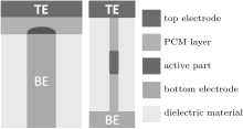
In2Se3 nanowires was synthesized[18] using vapor– liquid– solid technique with a diameter of 30 nm. The electrodes material was Pt and the insulator material was SiO2. As is shown in Fig. 1, conventional PCM[7] consists of a top electrode and a bottom electrode, the phase change material layer is sandwiched between the two electrodes. The nanowire-based PCM consists of a top electrode and a bottom electrode with the phase change material nanowire placed between the two electrodes, which is surrounded by dielectric material. Different from the conventional thin-film-based phase change memory, the active part of the phase change material is in the middle of the nanowire.
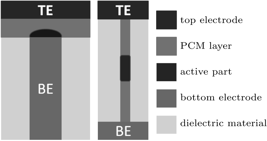 | Fig. 1. Schematic diagram of a conventional thin-film-based phase change memory device and NWs PCM. |
Figure 2 shows the measured resistance as a function of the variable RESET pulse amplitudes. Resistance for the initial crystalline state remains low until RESET pulse amplitude is close to 2.75 V, when PCM turns from low resistance state (LRS) to the high resistance state (HRS). ANSYS was used to simulate the temperature and amorphous distribution after the RESET operation. The corresponding parameters are listed in Table 1. Figure 3(a) shows the simulated temperature distribution within a nanowire-based memory device during 2-V RESET pulse. From the results, we can see that the highest temperature region is in the middle of the nanowire structure, which is 1227 K above the melting point (Tm= 953 K[21]) of In2Se3 material. Figure 3(b) shows the corresponding formed amorphous region (a-In2Se3). In nanowire-based PCM, LRS is usually considered as a complete crystalline region through the whole nanowire and HRS is related to a certain formed amorphous region inside the nanowire. When the RESET pulse amplitude increases from 2 V to 3 V, the thickness Ua of centralized amorphous region grows from around 50 nm to 100 nm, as illustrated in Figs. 3(b) and 3(c).
 | Fig. 2. Measured resistance with increasing RESET pulse amplitude for the cell in the initial crystalline state. |
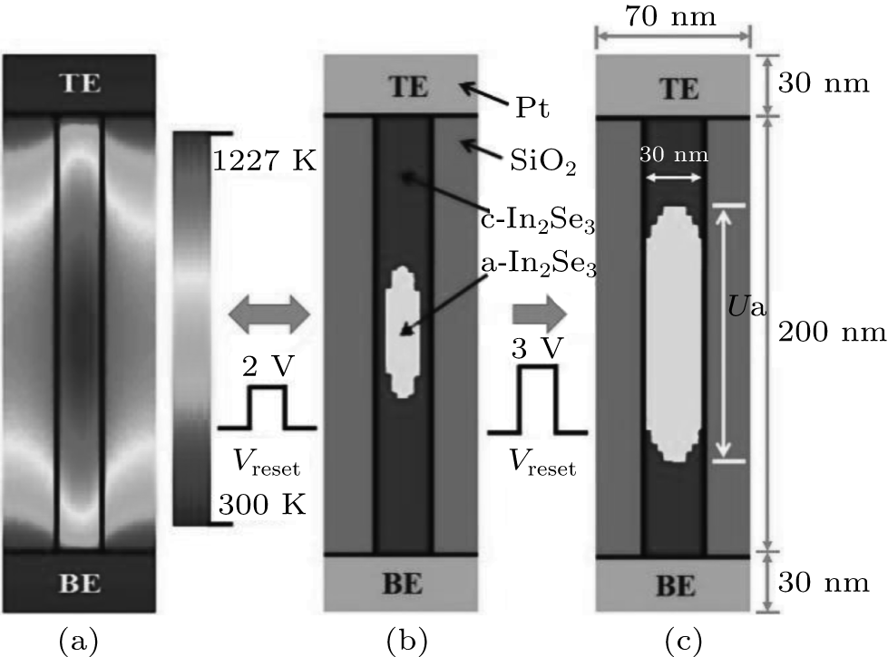 | Fig. 3. (a) Simulated temperature distribution in a nanowire-based memory device with 2-V RESET pulses and (b) the corresponding phase distribution. (c) Amorphous thickness Ua grows as the RESET pulse amplitude increases to 3 V. |
| Table 1. Parameters used in the simulation. |
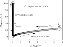
Figure 4 shows the measured I– V characteristics of amorphous state and crystalline state. The amorphous state and crystalline state have large resistance contrast below the threshold voltage Vth and shows electronic threshold switching behavior at Vth with the corresponding threshold current Ith. Threshold is defined as the point where the amorphous state is turned into the crystalline state inside the nanowire. In order to investigate the uniformity of the threshold voltage and current in In2Se3 nanowire-based PCM, multiple RESET operations are accomplished first to obtain the amorphous states and the I– V characteristics are measured to collect the values of threshold voltage Vth and threshold current Ith. The extracted values of Vth and Ith are shown in Fig. 5.
 | Fig. 4. Measured I– V characteristics of amorphous state and crystalline state. |
 | Fig. 5. The extracted threshold voltage Vth and threshold current Ith from multiple I– V measurements. |
Weibull cumulative distribution is introduced to describe the uniformity of the extracted Vth and Ith. Figure 6 shows a single slope of the Vth cumulative probability linear fitting with the value β = 3.8. However, two separated Ith cumulative probability linear fitting slopes are observed in Fig. 7 with values β 1 = 0.9 and β 2 = 7.5, respectively. The larger slope means that the distribution of the threshold is more centralized and the uniformity is better, while the smaller slope means that the uniformity is worse. Compared to that of the threshold voltage, the uniformity issue of the threshold current seems to be more complicated, and the mechanism behind this phenomenon will be discussed in the following section.
 | Fig. 6. Experimental data for the Weibull cumulative distribution of the extracted threshold voltage. |
 | Fig. 7. Experimental data for the Weibull cumulative distribution of the extracted threshold current. |
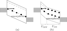
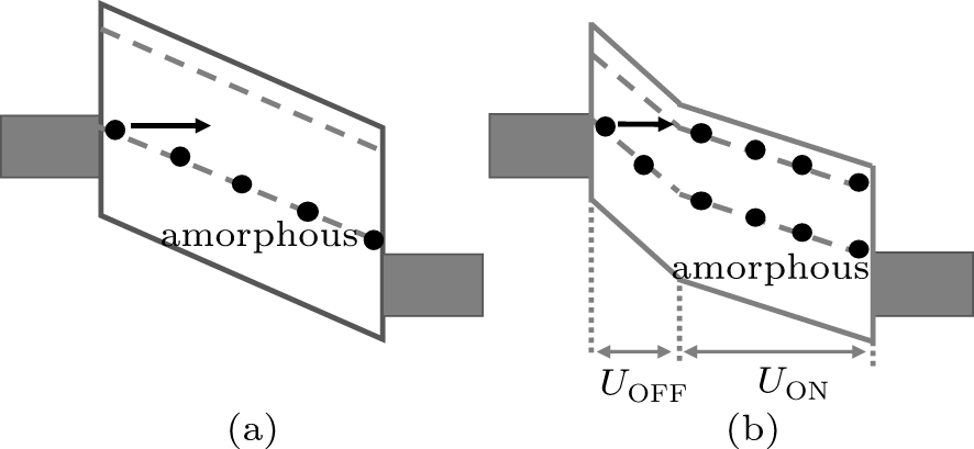
According to the trap-limited transport model[22, 23] proposed in the conduction in the amorphous state, carriers are thermally emitted from one trap to the conduction band and then captured by another trap which is commonly referred as the Poole– Frenkel transport. When a voltage is applied, the potential barrier to be overcome is decreased in the direction parallel to the electrostatic force as shown in Fig. 8. Figure 9 shows the carriers and traps distributions in the sub-threshold region, the trap filling obeys to the equilibrium conditions. High electrical field condition in the amorphous state can lead to a non-equilibrium distribution of carriers and injection of electrons into high energy states requires a certain distance UOFF, given by[22]

where q is the elementary charge, Et is the trap depth, and FOFF is the electric field in the OFF layer, given by

where A is the area of the contact, t0 is the characteristic attempt-to-escape time for the trapped electron, γ is the non-equilibrium term, Nt is the trap density, I is the current. As for the ON layer, the distance UON can be expressed by

where Ua is the total amorphous layer thickness. The related electric field in the ON layer can be written as

The non-uniformity of the electric field is essential to account for the threshold voltage switching. The voltage across the device is given by

 | Fig. 8. (a) Schematic diagram showing the electron trapped in the localized states at the trap depth Et. The inter-trap spacing is Δ z. (b) When applying an electric field, the barrier height is decreased. |
 | Fig. 9. Schematic diagram for the low-current (a) and high-current (b) potential profile and energy distribution of electrons in the amorphous state. |
According to the trap-limited transport model discussed above, electrons transfer via thermal emission over the potential barrier from one trap to the conduction band and then are captured by another trap in the amorphous state. Amorphous layer thickness Ua is one of the key factors in the conduction mechanism.[24] The trap depth Et determines the activation energy the carriers need to hop from one trap to another and the value can be decreased by applying an external voltage.[25] Especially, the different trap depths in the ON and OFF layers have a direct influence on the switching phenomenon, thus the switching voltage Vth and current Ith. Besides, the trap density Nt is another useful parameter which determines the trap distribution and spacing.[26] The three parameters, (Ua, Nt, and Et) have a major relationship to the uniformity of Vth and Ith and each parameter should be investigated separately to clarify its contribution.
As for the parameter Ua, a series of I– V characteristic simulations with input Gaussian distribution parameters Ua are accomplished firstly. Then, the Weibull cumulative distribution is used to study the amorphous layer thickness influence on the switching uniformity issues. The same analysis method can be applied to analyzing Nt and Et.
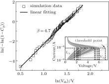
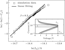
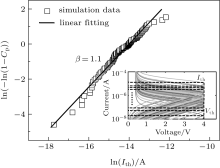
The simulated results are illustrated in Figs. 10– 12. The insets show the simulated I– V characteristics for the amorphous state using the Gaussian distribution parameters Ua, Nt, and Et, respectively. As is shown in the inset in Fig. 10, although the amorphous layer thicknesses are different, all the I– V curves have the same switching Ith while a variation of the Vth. The Vth Weibull cumulative distribution is shown with the linear fitting of only one slope with β = 4.7. From the inset in Fig. 11, contrary to Ua, the variation of trap density Nt has no effect on the Vth but slight effect on the Ith. The linear fitting of Ith Weibull cumulative distribution shows only one slope with β = 8.2. Similar to Nt, the variation of Et has the same effect on the Vth and Ith, but with a smaller slope β = 1.1 (see Fig. 12). Based on the simulation results, we can make a conclusion that amorphous thickness Ua is the basic factor that leads to the uniformity of Vth. Both the two factors (trap density Nt and trap depth Et) can directly change the critical threshold electrical field that determines the Ith which contributes little to Vth. The two slope values β = 8.2 and β = 1.1 indicate that the variation of Et contributes more to the uniformity of Ith. The simulation results also have a clear explanation of the experimental data in Figs. 6 and 7.
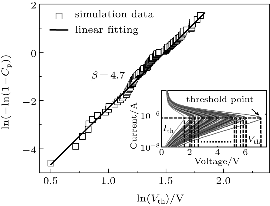 | Fig. 10. Weibull cumulative distribution of Vth with linear fit (slope β = 4.7). The inset shows I– V characteristics for the amorphous state using the Gaussian distribution data of the amorphous layer thickness Ua. |
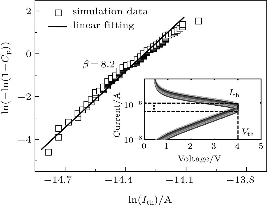 | Fig. 11. Weibull cumulative distributionof Ith with linear fit (slope β = 8.2). The inset shows I– V characteristics for the amorphous state using the Gaussian distribution data of the trap density Nt. |
 | Fig. 12. Weibull cumulative distribution of Ith with linear fit (slope β = 1.1). The inset shows I– V characteristics for the amorphous state using the Gaussian distribution data of the trap depth Et. |
In this paper, the extracted threshold voltage Vth and current Ith of the nanowire-based In2Se3PCM were collected and the Weibull cumulative distribution was studied to investigate the threshold uniformity characteristics. Based on the trap limited model, factors (amorphous layer thickness Ua, trap density Nt, and trap depth Et) were used to clarify their influences upon the switching parameters Vth and Ith. We conclude that the uniformity of Vth is mainly caused by the variation of the amorphous thickness which has little effect on the Ith. On the contrary, uniformity of the threshold current is largely induced by the trap density and trap depth while the latter influence is more sensitive. Our conclusion is of great use for designing the devices with a certain range of maximum programming voltage and current, especially for the low voltage devices.
| 1 |
|
| 2 |
|
| 3 |
|
| 4 |
|
| 5 |
|
| 6 |
|
| 7 |
|
| 8 |
|
| 9 |
|
| 10 |
|
| 11 |
|
| 12 |
|
| 13 |
|
| 14 |
|
| 15 |
|
| 16 |
|
| 17 |
|
| 18 |
|
| 19 |
|
| 20 |
|
| 21 |
|
| 22 |
|
| 23 |
|
| 24 |
|
| 25 |
|
| 26 |
|