1. IntroductionAlGaN/GaN heterostructure field effect transistors (HFETs) grown on Si substrate by metal organic chemical vapor deposition (MOCVD) are very promising in commercial applications of RF power devices and high-power switch devices. This is attributed to advantages of the high two-dimensional electron gas (2DEG) density and the high breakdown field of GaN-based materials, combined with the low manufacturing cost of Si substrates. Semi-insulating or high-resistivity GaN (HR-GaN) is essential for AlGaN/GaN HFETs to decrease parallel conduction between drain and source and to ensure a good pinch-off of the channel. The unintentional doped HR-GaN buffer has been achieved by introducing higher edge-type dislocation to compensating the n-type background residual donor.[1– 3] The off-state performance of HFETs fabricated on these HR-GaN buffer layers encountered a bottleneck for further leakage current reducing, due to the poor confinement of the 2DEG, which could cause a much more serious problem when the gate length (Lg) of HFET decreases for higher frequency operation of the transistors.[4, 5] The introduction of back barrier structures beneath the 2DEG channel, such as the AlGaN/GaN/AlGaN double-heterostructure and Mg-doped GaN buffer layer, [6– 8] have been proved to be a very effective way to enhance carrier confinement with much lower leakage current. However, both a thick AlGaN back barrier layer and Mg-doped GaN would easily result in poor crystal quality, degradating the 2DEG channel layer grown subsequently. In addition, thick and heavy Mg-doped GaN would cause a serious memory effect of Mg atoms.[9– 11] Thus, the output current densities of the fabricated HFETs were deteriorated correspondingly.
Therefore, both good output and pinch-off properties were expected in the HFETs grown on Si substrate. Here, a novel HFET structure was proposed, in which a very thin Mg-doped GaN (Mg– GaN) and Si-doped GaN (Si– GaN) pair-doped interlayers are inserted (see Fig. 1(a)). The thin Mg– GaN grown here not only ensures lower leakage current, but also weakens the memory effect of Mg atoms. The Si– GaN interlayer is necessary for compensating for the excess Mg[12] due to the memory effect[13] and preventing the 2DEG from depleting. It has also been reported that both proper Si- and Mg-doped concentrations in GaN or AlGaN can improve the structural quality.[14– 16] In this experiment, by optimizing the doping concentrations of the pair-doped interlayers, the off-state performance improved significantly without sacrificing the output characteristics. The correlation between the material characteristics and device performance provides insight understanding of the mechanisms that improve electrical characteristics in HFETs.
2. ExperimentA conventional undoped AlGaN/GaN HFET structure was grown as a reference (B0 in Table 1) on Si(111) substrate by MOCVD, which consists of a 30-nm high-temperature AlN buffer layer, a 1.6-μ m HR-GaN layer with insertion of two low temperature grown AlN interlayers for strain engineering, [17] and finally a 25-nm AlGaN barrier layer with ∼ 30% Al composition. The proposed HFET with the Mg– GaN and Si– GaN interlayers, which were inserted beneath the 40 nm GaN channel
(see Fig. 1(a)), were grown under the same growth conditions with the conventional structure except for different dopant flow rates. In the proposed HFET, the doping level of both the Si and Mg-doped interlayer reduced simultaneously to keep the Cp2Mg/SiH4 ratio as a constant of 20. Here we introduced the relative doping concentration (RDC) to represent the doping level, in which RDC-0, RDC-1, RDC-2, and RDC-4 represented B0, B1, B2, and B4 from the undoped to the higher doping level, respectively. Meanwhile, HFET devices and Schottky diodes were also fabricated, in which the Ti/Al/Ni/Au were deposited for ohmic contact with electron-beam evaporation and annealed at 830 ° C for 30 s in nitrogen ambient and the Ni/Au was deposited for Schottky contact. The I– V performance was measured by an Agilent B1505A. The HFETs discussed here are all in the same dimension with Lg, Lgs, Lgd, and Wg values of 3, 3, 5, and 100 μ m, respectively.
3. Results and discussionFigure 1(b) shows the secondary ion mass spectrometry (SIMS) profile of Mg and Si atoms concentration in sample B1. The position mark A and A1 indicate that the Cp2Mg and SiH4 sources were switched on, respectively. Due to the tiny Mg-doped concentration, the Mg profile delay tail (Mg memory effect) only extended about 30 nm (section AA2 in Fig. 1(b)), which is 20 nm away from the 2DEG channel. While the higher Si signal in the initial stage (at the surface of the structure) of B1 is affected by the surface Si pollution and the Silicon concentration for B0 shows nearly the same level at the surface (SIMS data not shown here) which may be due to the contamination from the atmosphere after growth. The introduction of Si below the channel could effectively compensate for the excess Mg[12] due to the memory effect, [13] which made a Si and Mg co-doped interlayer exist here. In this co-doped region, the conduction band diagram of the proposed HFET is shown in the inset of Fig. 1(b). This increased barrier height is assumed to effectively prevent the leakage current through the buffer layer beneath the channel layer.
Table 1.
Table 1.
 Table 1. Material characteristics and device properties of samples with various doping concentration levels. | (Cp2Mg/TMGa)/10− 4 mol/mol | SiH4/TMGa/10− 5 mol/mol | Cp2Mg/SiH4/mol/mol | RDC | XRD FWHM/arcsec | PL | Hall mobility/cm2· V− 1· s− 1 | AFM RMS @5 μ m/nm | IDmax/mA· mm− 1 | Ron/Ω · mm |
|---|
| | | | 002 | 102 | Peak/eV | FWHM/meV | 300K | 5 K | | | |
|---|
| B0 | – | – | – | 0 | 580 | 1090 | 3.401 | 41.8 | 1060 | 4095 | 0.56 | 718 | 5.6 | | B1 | 1.5 | 0.75 | 20 | 1 | 602 | 1079 | 3.399 | 37.3 | 1200 | 7920 | 0.26 | 792 | 4.6 | | B2 | 3 | 1.5 | 20 | 2 | 592 | 1093 | 3.397 | 41.9 | 985 | 5520 | 0.29 | 553 | 5.8 | | B4 | 6 | 3 | 20 | 4 | 583 | 1113 | 3.379 | 100.7 | 539 | 1360 | 0.55 | 342 | 12 |
| Table 1. Material characteristics and device properties of samples with various doping concentration levels. |
Room-temperature Hall measurement (Table 1) indicates that the conduction property improves with the RDC reducing from 4 to 1. The mobility of sample B1 reaches 1200 cm2/V· s, which is superior to that of undoped sample B0. Furthermore, the temperature-dependent Hall effect measurements were carried out on these samples (see Fig. 2). The sheet carrier density of the investigated samples does not show any appreciable change (see Fig. 2(c)). The temperature-dependent electron Hall mobility in Fig. 2(a) shows that when the temperature drops to 5 K, the electron mobility of samples B2 and B1 reaches 5520 and 7920 cm2/V· s respectively, which is significantly higher than that of a conventional sample (4095 cm2/V· s). These phenomena indicate that the scattering becomes weak under lower temperatures. Several scattering mechanisms affect the electron mobility of 2DEG, and the separation of their contributions is usually performed through temperature-dependent measurement.[18– 20] At high temperature (above 100 K), electron mobility decreases with increasing temperature, which is a typical temperature dependent of phonon scattering mobility. However, the low-temperature (below 100 K) electron mobility keeps almost the same, which is dominated by temperature-independent scattering factors, such as the interface roughness, alloy disorder, charged defect scattering and ionized impurity scattering. On one hand, in our experiments all the samples were grown under the same MOCVD condition except the different dopant flow rates in pair-doped interlayers. Therefore, the alloy disorder scattering effect should remain the same in all the investigated samples. On the other hand, a relatively low RDC (B1) sample can lead to a growth condition with less charged defect scattering center, which can improve the mobility. Meanwhile, the sample with relative low RDC pair-doped interlayers and a 30 nm unintentionally doped GaN channel layer can minimize the influence of the ionized impurity scattering. However, the ionized impurity scattering can play a more important role on the reduction of the mobility in the relatively high RDC sample (B4). The discussion above is the reason why the mobility varies from B0 to B4 as shown in Fig. 2(a). Furthermore, according to the well-known equation ρ = 1/enμ and the discussion above, we can easily understand why the sheet resistivity varies from B0 to B4 as shown in Fig. 2(b). All in all, the different doping level related channel crystal quality and interface roughness will be the key factors responsible for the improvement in electron mobility under low temperature.
High-resolution x-ray diffraction (XRD) measurements were carried out to characterize the crystal quality and the influence of the Si/Mg interlayers on the strain state of the epilayer. As shown in Table 1, the FWHMs of (002) and (102) rocking curves of the investigated sample are all around 600 arcsec and 1100 arcsec, respectively, which is independent of the change of RDC. As we know, the detection depth of the XRD measurement can reach several hundred nanometers. This means that the FWHMs of (002) and (102) mainly reflect the crystal quality of the HR-GaN of the investigated samples, in which all the epilayers beneath the Si/Mg pair-doped interlayers in this work are grown in the same condition. Meanwhile, by measuring XRD reciprocal space maps (RSM) of the (105) reflections (not shown here), it is found that the AlGaN peaks of all the samples were perfectly aligned with the main GaN peak vertically, indicating that the insertion of the Si/Mg interlayers has no influence on the strain state of the AlGaN barrier layer and the GaN buffer layer. In order to evaluate the crystal quality around the channel, the room-temperature PL spectrum is recorded, which are very different from each other in Fig. 3, in which the topmost GaN layer mainly contributes to the luminescence. The spectra of all samples display intense band edge transition (∼ 3.4 eV), while the IBE/IBE0 intensity ratio (the band edge transition intensity for proposed samples to that of conventional sample B0) increases significant by a factor of 4.3 in sample B1. The highest luminescence intensity and best PL FWHM value of band edge transition (see Table 1) in sample B1 is attributed to good suppression of nonradiative transitions, whose recombination rate is proportional to the density of native defects.[21] Therefore, in sample B1 with the lowest Si and Mg dopant levels, the nonradiative related defects near the GaN channel layer reduce significantly in comparison with undoped or higher doped samples. Combining the PL with the Hall mobility results, a good correlation is observed with higher electron mobility as the band edge emission increases (see the inset in Fig. 3). It can be deduced that the quality of GaN near the 2DEG channel in the pair-doped interlayer improves with a lower density of defects, which may play an important role in the charged defect scattering.
In addition, it should be noted that the interface roughness would also be very sensitive to the Hall mobility of 2DEG. A clear step-flow growth surface is observed with all the samples, with the terrace width varying from 50 nm to 100 nm (not shown here). The surface root mean square (RMS) roughness values of these four samples are extracted and listed in Table 1, in which the sample B1 has the smoothest surface with an RMS of 0.26 nm. This means the adsorption of Si or Mg atoms on the growth surface, which act as surfactants, appears to enhance the surface mobility of the group-III atoms. However, the increase of RMS value in sample B4 with higher SiH4 and Cp2Mg flow rates may be ascribed to the increase of dislocation density.
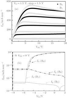
The improvements in the conduction properties have also been verified by the HFETs device performance. The maximum drain current values IDmax and conduction resistance Ron were extracted from the output I– V properties and are shown in Table 1. When the doping concentration decreases, the output performance improves gradually and reaches the largest IDmax (792 mA/mm) in sample B1, which increases by 10% in comparison with that of conventional sample B0 (see Fig. 4(a)). Moreover, from the transfer characteristic (see Fig. 4(b)), it can be observed that the off-state channel leakage current was limited by the Schottky reverse leakage current in the gate region. The off-state drain leakage current density Id reaches as low as 2.2 × 10⁷ in sample B1, which is about four orders lower in magnitude than that of B0. This ultralow off-state channel leakage current, which is limited by the Schottky reverse leakage current, makes the current on/off ratio reach as high as 3.6 × 10⁹ in sample B1.
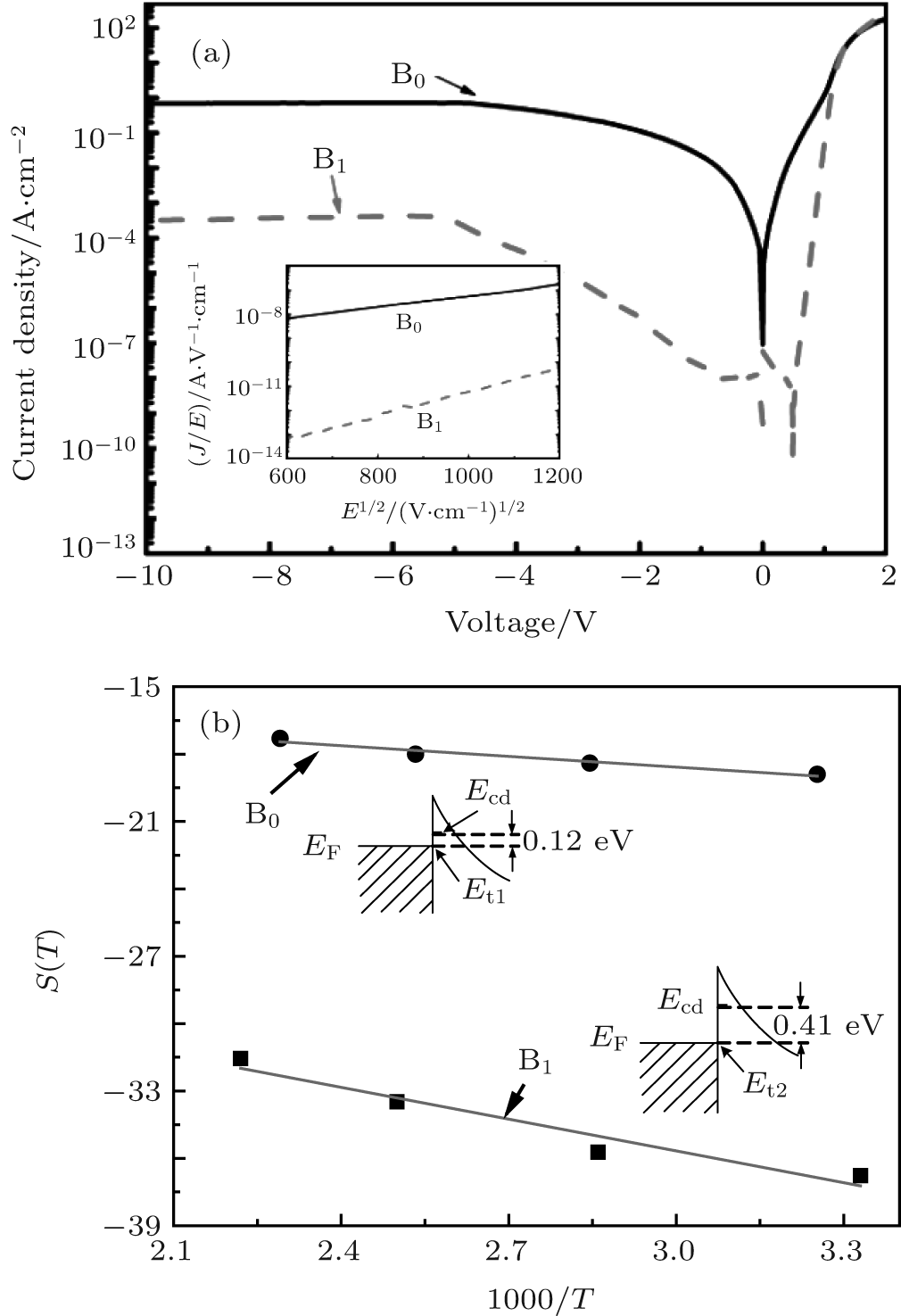
Therefore, in order to explore the mechanisms for the improvement in off-sate leakage current, Schottky diodes were also fabricated and characterized. Figure 5(a) shows the I– V characteristics of the Schottky diode in samples B0 and B1. The forward characteristic of B1 is more ideal than that of B0, due to the higher slope in the log-scale plot. Meanwhile, a much lower reverse leakage current is also observed in B1 in comparison with B0. Specifically, as shown in the inset of Fig. 5(a), we observe a linear dependence of ln(J/E) on  under the reverse-bias condition for both diodes, where J is the current density and E is the electric field in the semiconductor barrier. This indicates that the reverse leakage current is dominated by the Frenkel– Poole emission.[22] At room temperature, the carrier transport via conductive dislocations is the dominant source of reverse leakage currents in the Schottky contacts to the n-type nitride semiconductor material.[22– 24] It is suggested that the key process in reverse leakage current flow is the emission of electrons from a trap state near the metal-semiconductor interface into a continuum state associated with the conductive dislocation.
The current density associated with Frenkel– Pool emission is given by[22, 25, 26]

where Φ t is the barrier height for the electron emission from the trapped state, ε s is the relative dielectric permittivity, ε 0 is the permittivity of free space, T is the temperature, and k is Bolzmann’ s constant.
In Eq. (1), ln(J/E) should be a linear function of , i.e.,

As seen in the inset of Fig. 5(a), the leakage current densities are well described by the electric field dependence of Eq. (2).
Furthermore, the emission barrier height (Φ t) values for the Schottky diode can be extracted from these data values. We measured the reverse leakage current from 300 K to 450 K. From the slope of S(T) versus 1/T shown in Fig. 5(b), we obtain Φ t values with 0.12 eV and 0.41 eV for samples B0 and B1, respectively. We assume that the trapped state (Et1 and Et2 for samples B0 and B1, respectively) should be close to the metal Fermi level[22] due to the pinning effect, as shown in both insets of Fig. 5(b). In both samples, the conductive dislocations (Ecd) are approximately in the same level of energy, as required for the conduction along dislocation lines across heterojunction interfaces. Thus, the relevant trapped state would be located 0.12 eV and 0.41 eV below the conductive dislocation level (Ecd) for samples B0 and B1, respectively. It is believed that the effective barrier height (Φ eff) in the Schottky diodes of B1 would also be much higher than that of B0, which benefits from a higher emission barrier height. We speculated that the inhibition of shallow surface traps should be the main reason for the good suppression of reverse leakage current in sample B1. This phenomenon is also consistent with the PL results, which confirms that the trap densities and surface states would seriously affect the device performance.


 ]
]