
Enhanced surface plasmon interference lithography from cavity resonance in the grating slits*
[Guo Kai, Liu Jian-Long, Zhou Ke-Ya, Liu Shu-Tian† ]
]
]
 |


†Corresponding author. E-mail: stliu@hit.edu.cn
*Project supported by the National Basic Research Program of China (Grant No. 2013CBA01702) and the National Natural Science Foundation of China (Grant Nos. 61377016, 61308017, and 61307072).
Surface plasmon interference lithography based on grating diffraction has been studied both theoretically and experimentally in recent years. In this paper, we demonstrate that the cavity resonance in the grating slits can improve the subwavelength interference, not only the intensity but also the uniformity of the pattern. Both the typical lithography structure which merely consists of periodic metallic gratings and the modified structure equipped with a reflection layer are studied. The finite element method has been performed to study the interference pattern. Numerical simulations show that the property of the interference pattern is the optimum when cavity resonance happens. This enhancement can be applied to all the lithography structures which are based on the grating diffraction.
As nanoscale science and technology develop rapidly, the fabrication of a nano-pattern is urgently required. To achieve a smaller nano-pattern beyond the diffraction limit, reducing the working wavelength[1– 4] and increasing the numerical aperture[5– 7] are two straightforward methods. However, the shortcomings, including the complexity and the great cost of the instruments and processing, restrict their applications. Surface plasmon interference lithography (SPIL) is one of the recent developed lithography technologies. It attracts much attention because it can achieve subwavelength pattern[8– 11] with short exposure time due to the local field enhancement in plasmonic structures.
To promote the application of the SPIL technology in the industry, some modified structures and methods have been proposed.[12– 17] Some difficulties, however, still remain. The light intensity transmitted through the masks is weak despite the enhanced optical transmission (EOT) by the surface plasmons (SPs). Therefore, an efficiently high exposure intensity is required to fabricate patterns. In addition, the SPs decay along the metal/dielectric interface, leading to a non-uniformity of the interference pattern in the exposure area.
Recently, a closed structure, consisting of a metallic grating and a cladding layer, is used to realize ultra-deep subwavelength photolithography.[12, 15] In this structure, the interference zone can be treated as an SPs resonant cavity. Li et al. analyzed the function of this kind of SPs cavity and its effect on enhancing the photolithography.[17] This SPs cavity has been extended to super-resolution imaging of two-dimensional patterns.[18] However, this kind of SPs resonant cavity can only be employed in the closed structure.
In this work, the cavity resonance in the grating slits is analyzed and applied to improve the performance of subwavelength interference, not only the intensity but also the uniformity of the interference pattern. Simulations are done under two schemes: (i) the typical open structure which merely consists of periodic metallic gratings; (ii) the closed structure equipped with a metal cladding layer. The results indicate that the property of the interference pattern can be modulated by tuning the thickness of the grating and the width of the slit. Moreover, the interference pattern is significantly optimized under cavity resonance.
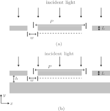
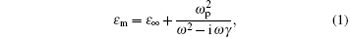
The schematics of the two SPIL structures are presented in Figs. 1(a) and 1(b), respectively. The slit width, the period, and the thickness of grating are denoted by w, p, and L, respectively. In Fig. 1(b), the spacing between the grating and the metal reflection layer is denoted by h.
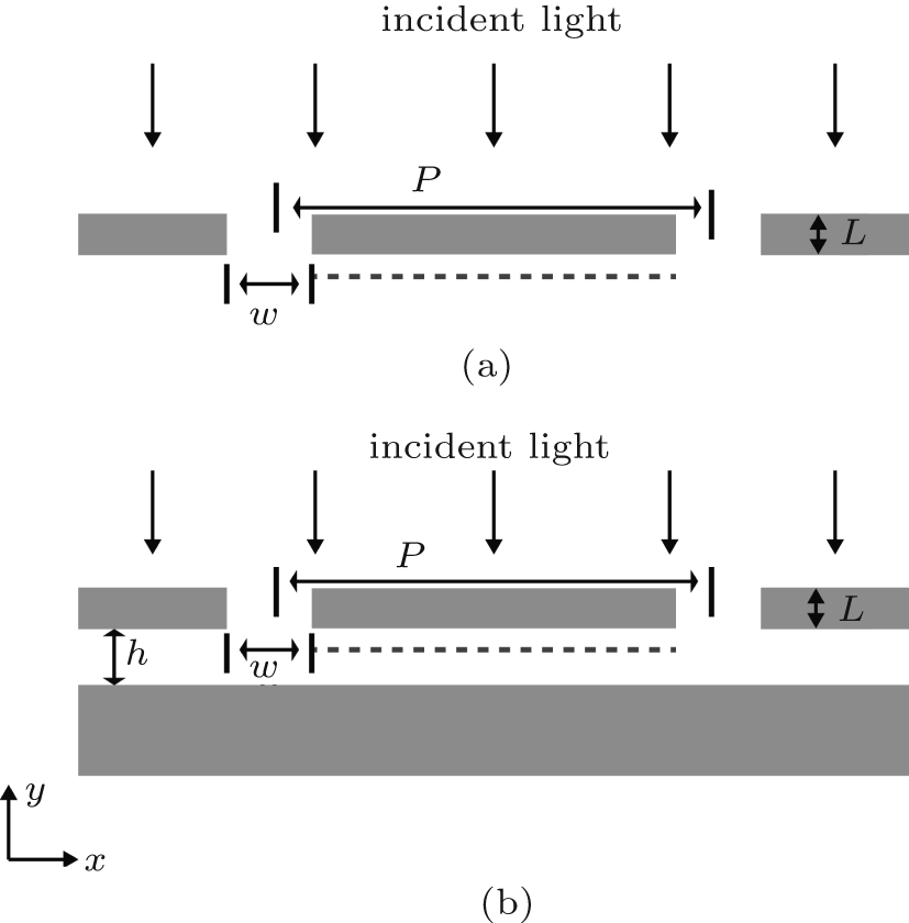 | Fig. 1. Schematics of the SPs interference performed in simulation. (a) Open structure and (b) closed structure. |
The metal we used in the simulation was silver and described by the Drude model,
where ε ∞ = 4.2 is the high frequency permittivity, ω p = 2.2 × 10¹⁶ rad/s is the plasma frequency, γ = 9.1 × 10¹³ rad/s is the collision frequency.[12] In this paper, ε Ag = − 2.1348 + 0.1116i with incident wavelength λ 0 = 365 nm. For the sake of simplicity, we consider air as the dielectric: ε 0 = 1. The metal and air are treated to be nonmagnetic under TM-polarized light.
The finite element method is adopted to do the numerical simulation. The field intensity is evaluated by the maximum peak of the interference pattern, and the uniformity is defined as the ratio of the minimum value to the maximum value of the interference peaks. The values of the interference peaks are extracted along a cut line (shown in Figs. 1(a) and 1(b) with dashed lines) which is 30 nm below the metallic grating.
When a TM-polarized light is normally incident upon the periodic metallic grating, it will be partly trapped into the slits. Thus, SPs will be excited inside the slits. The slits can be regarded as SPs cavities if the space between neighboring slits is large enough. The effective refractive index neff in the cavity can be calculated from the following dispersion equation[19]
where k0 is the wave-vector in free space, and β = neffk0 is the propagation constant in the cavity. ε m(d) denotes the permittivity of the metal (dielectric), respectively.
Note that only TM modes are taken into consideration due to the nature of SPs modes excited on the interface between the metal and the dielectric.[20] For SPs modes, the relation between the electric field and the magnetic field can be written as 
The light passing through the slit will diffract at the lower surface of periodic grating. The wave-vector of diffraction light can be described as kx = 2nπ /p (n = 1, 2, 3, … ). For the open structure, SP resonance will be excited at the lower surface of gratings if the matching relation 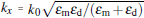
The field intensity below the grating will be enhanced when the cavity resonance condition is satisfied[22]

where m is an integer, and ϕ is the phase shift of SPs at both ends of the cavity. According to Eq. (2) and Eq. (3), the interference field intensity can be modulated by tuning the slit width w and grating thickness L. The interference pattern, including the field intensity and uniformity, can be improved by optimizing the geometric parameters. To support our analysis, the characteristics of the interference pattern will be numerically studied and discussed based on two interference schemes in the following.
In the open structure (shown in Fig. 1(a)), the lower grating surface can be approximately treated as the interface between semi-infinite metal/dielectric. When λ 0 = 365 nm, ksp = 1.3694k0. According to the matching relation, the grating period is p = 800 nm with an arbitrary chosen diffraction order n = 3.
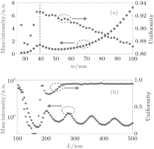
Figure 2(a) shows the field intensity and uniformity with various w and a fixed grating thickness L = 280 nm. When w increases from 30 nm to 40 nm, the field intensity and uniformity increase. When w increases from 40 nm, the uniformity decreases monotonously. The field intensity, after decreasing a little, increases rapidly with slit width. Taking w = 40 nm satisfies cavity resonance and enhances the interference pattern. The physical mechanism behind this phenomenon can be explained by Eq. (2). When w increases from 30 nm to 60 nm, neff of the cavity decreases from 2.7049 to 1.9168. When w is large enough, neff approaches a constant 1.3694. So with the width increasing, the phase changing caused by Δ neff is limited within 2π . Then as the width is varying, only one cavity resonance occurs at w = 40 nm. Moreover, a wider slit leads to more light passing and a higher field intensity.
 | Fig. 2. Maximum of the interference peak and the uniformity along the cut line (shown in Fig. 1) versus (a) the slit width w and (b) the grating thickness L. The unit a.u. means arbitrary units. |
With a fixed slit width w = 40 nm (neff = 2.3041), the dependence of the field intensity and uniformity on grating thickness L is depicted in Fig. 2(b). With L increasing, the intensity prohibits a periodic property and resonates around L = 110 nm, 200 nm, 280 nm, 360 nm, and 440 nm, respectively. The period is about 80 nm, which agrees well with the theoretical value obtained by Eq. (3). However, the uniformity does not behave as a periodic function of thickness. When L is large enough, the interference possesses a high level and stable uniformity.
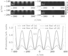
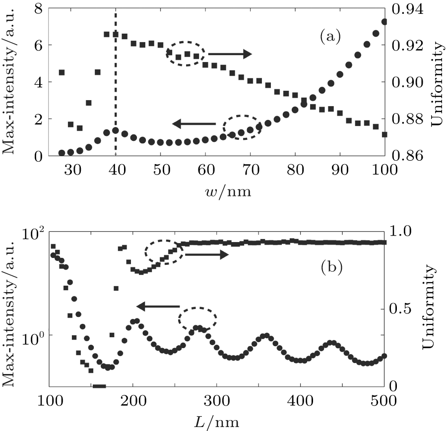
We present some field distributions under the grating in Figs. 3(a)– 3(d). The field distributions along the cut line are extracted and plotted in Fig. 3(e). Figures 3(a) and 3(b) are the results of the resonant case and a non-resonant case of Fig. 2(a), with L = 280 nm, w = 40 nm and L = 280 nm, w = 32 nm, respectively. Figures 3(c) and 3(d) show the field distribution of the resonant case and a non-resonant case of Fig. 2(b), with L = 360 nm, w = 40 nm, and L = 160 nm, w = 40 nm, respectively. Comparisons between Figs. 3(a) and 3(b), 3(c) and 3(d) demonstrate that the cavity resonance enhances the interference pattern, both the intensity and uniformity.
 | Fig. 3. Field distributions of | Hz| 2 in the x– y plane under grating for (a) L = 280 nm, w = 40 nm; (b) L= 280 nm, w= 32 nm; (c) L = 360 nm, w = 40 nm; (d) L = 160 nm, w = 40 nm. (e) Distributions along the cut line. |
In the closed structure (as shown in Fig. 1(b) above), the interference area under the grating can be regarded as a metal/dielectric/metal waveguide. The wave vector of the plasmon wave is ksp = 2.3041 k0 when h = 40 nm. The grating period p = 634 nm fulfills the matching condition with the arbitrarily chosen n = 4.
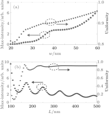
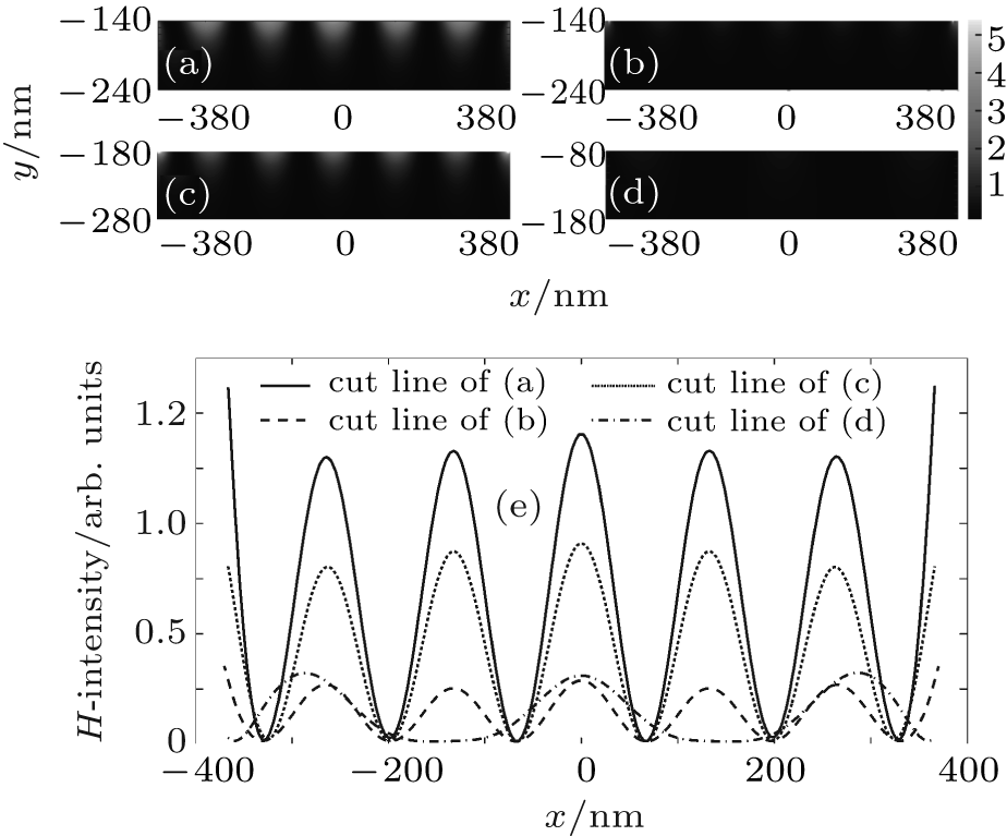
Figure 4(a) summarizes the field intensity and uniformity along the dashed cut line under various w with a fixed L = 320 nm. No significant cavity resonance appears on the two curves. Note that the upper exit of the slit is open, but the lower exit is covered by a metal reflection layer. Such an asymmetric cavity wall leads to the cavity effect in the slit being reduced. Nevertheless, a wider slit allows more light passing and leads to a higher intensity. The uniformity approaches a constant with the slit width w increasing. If the period is a constant, the wider slit cuts down the interference area. Consequently, less interference fringes can be achieved.
 | Fig. 4. Maximum of the interference peak and the uniformity along the cut line in Fig. 1 versus (a) the slit width w and (b) the grating thickness L. |
Given the slit width w = 40 nm, the dependence of field intensity and uniformity on the grating thickness L is shown in Fig. 4(b). When L increases, the field intensity prohibits the periodic property and the period agrees well with the theoretical value. Meanwhile, the uniformity reaches a high and steady level when L is large enough.
To support the results in Fig. 4, the field distributions under grating of some cases are presented in Figs. 5(a)– 5(d). The field distributions along the cut line are extracted and plotted in Fig. 5(e). From Fig. 4(a), we know that the cavity resonance is not sensitive to slit width with a fixed grating thickness. Nevertheless, to keep consistency, we show the results in Figs. 5(a) and 5(b) corresponding to Fig. 4(a), with L = 320 nm, w = 50 nm and L = 320 nm, w = 30 nm, respectively. Figures 5(c) and 5(d) show the field distribution of the resonant case and a non-resonant case of Fig. 4(b), with L = 250 nm, w = 40 nm and L = 290 nm, w = 40 nm, respectively. A comparison between Figs. 5(c) and 5(d) demonstrates that by giving a constant slit width w, resonant grating thickness enhances the property of the interference pattern.
 | Fig. 5. Field distributions of | Hz| 2 in the x– y plane for (a) L = 320 nm, w = 50 nm; (b) L = 320 nm, w = 30 nm; (c) L = 250 nm, w = 40 nm; (d) L = 290 nm, w = 40 nm. (e) Distributions along the cut line. |
In conclusion, the cavity resonance in the grating slits is proposed to enhance the subwavelength interference pattern with a high contrast and a good uniformity. Numerical study has been performed under two typical schemes. The simulation results show that the property of the interference pattern can be optimized by designing the grating thickness and slit width. Because the cavity resonance is formed inside the grating slit, it can be applied in all the lithography techniques which are based on grating diffraction.
| 1 |
|
| 2 |
|
| 3 |
|
| 4 |
|
| 5 |
|
| 6 |
|
| 7 |
|
| 8 |
|
| 9 |
|
| 10 |
|
| 11 |
|
| 12 |
|
| 13 |
|
| 14 |
|
| 15 |
|
| 16 |
|
| 17 |
|
| 18 |
|
| 19 |
|
| 20 |
|
| 21 |
|
| 22 |
|