Zhou Tian-Yu, Liu Xue-Chao, Huang Wei, Dai Chong-Chong, Zheng Yan-Qing, Shi Er-Wei. Application of an Al-doped zinc oxide subcontact layer on vanadium-compensated 6H–SiC photoconductive switches* . Chinese Physics B, 2015, 24(4): 044209
Permissions
Application of an Al-doped zinc oxide subcontact layer on vanadium-compensated 6H–SiC photoconductive switches*
Zhou Tian-Yua),b), Liu Xue-Chaoa)†, Huang Weia), Dai Chong-Chonga),b), Zheng Yan-Qinga), Shi Er-Weia)
Shanghai Institute of Ceramics, Chinese Academy of Sciences, Shanghai 201800, China vglue2pt
University of the Chinese Academy of Sciences, Beijing 100049, China
*Project supported by the Innovation Program of the Shanghai Institute of Ceramics (Grant No. Y39ZC1110G), the Innovation Program of the Chinese Academy of Sciences (Grant No. KJCX2-EW-W10), the Industry–Academic Joint Technological Innovations Fund Project of Jiangsu Province, China (Grant No. BY2011119), the Natural Science Foundation of Shanghai (Grant No. 14ZR1419000), the Young Scientists Fund of the National Natural Science Foundation of China (Grant No. 61404146), and the National High-tech R & D Program of China (Grant Nos. 2013AA031603 and 2014AA032602).
Abstract
Al-doped ZnO thin film (AZO) is used as a subcontact layer in 6H–SiC photoconductive semiconductor switches (PCSSs) to reduce the on-state resistance and optimize the device structure. Our photoconductive test shows that the on-state resistance of lateral PCSS with an n+-AZO subcontact layer is 14.7% lower than that of PCSS without an n+-AZO subcontact layer. This occurs because a heavy-doped AZO thin film can improve Ohmic contact properties, reduce contact resistance, and alleviate Joule heating. Combined with the high transparance characteristic at 532 nm of AZO film, vertical structural PCSS devices are designed and their structural superiority is discussed. This paper provides a feasible route for fabricating high performance SiC PCSS by using conductive and transparent ZnO-based materials.
Photoconductive semiconductor switches (PCSSs) are semiconductor devices that can achieve on- and off-states by controlling the generation and recombination of carriers in semiconductor material through laser triggering. They can be used in high power systems, such as pulsed power systems and ultra-wideband source systems.[1– 3] A compact dielectric wall accelerator (DWA) is regarded as one of the most promising applications. The key components for a compact DWA are high performance switches, high gradient insulator, and asymmetric Blumlein pulse forming line.[4] PCSS is considered to be the ideal switch for a compact DWA system due to its lower jitter time, faster response, and smaller volume, compared to a traditional spark gap switch.
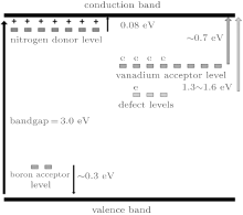
Silicon (Si) and gallium arsenide (GaAs) materials have attracted great attention in fabricating PCSS devices.[5– 7] However, despite the rapid progress in Si and GaAs PCSSs, the device performance is strictly limited by the intrinsic material properties, especially at extreme conditions. The dark current in Si PCSS is not negligible when operating at high voltage bias, due to the low resistivity of Si. Although GaAs shows better breakdown voltage tolerance than Si, its low thermal conductivity restricts its application in high power systems. Poor heat dissipation characteristics can lead to earlier thermal failure of PCSS at elevated temperatures. Silicon carbide (SiC) is regarded as a candidate material for fabricating high performance PCSS used in harsh environments due to its high thermal conductivity (4.9 W· cm− 1· K− 1), high breakdown field (3.0 MV/cm), large saturation electron velocity (2.0 × 107 cm/s), and wide band gap (6H– SiC: 3.0 eV, 4H– SiC: 3.2 eV, 3C-SiC: 2.2 eV). In particular, 6H– SiC can achieve a semi-insulating characteristic via vanadium doping, which is crucial for high power PCSSs. Vanadium dopant is an amphoteric impurity which can act as either a donor or an acceptor. In the case of the 6H– SiC that we have used, vanadium serves as a deep acceptor (0.7 eV below the conduction band) when the nitrogen impurity (shallow donor level: 0.08 eV below the conduction band) density exceeds the boron impurity (shallow acceptor level: 0.3 eV above the valence band) density.[8, 9] Thus the Fermi level can be pinned close to the vanadium acceptor level, which results in the semi-insulating nature of vanadium-compensated 6H– SiC. Figure 1 presents the extrinsic levels contained in vanadium compensated 6H– SiC.[10] Moreover, the inter-band impurities and dopants in vanadium-compensated semi-insulating 6H– SiC (VCSI 6H– SiC) can also be effectively utilized when the vertical PCSS is triggered at below band gap wavelengths.
SiC PCSS attracted much attention in the past decade due to the notable progress in SiC bulk material, however, most of these studies have focused on improving the hold-off characteristic of PCSS, both in experiments and theoretical simulations.[11– 13] Few studies have focused on concrete ways to optimize the structure and to reduce the on-state resistance of PCSSs. Large on-state resistance results in high thermal loss from a PCSS and decreases the system’ s output power. An optimized structure can facilitate device integration and improve performance. Thus, reasonable device structure and reduced on-state resistance are still worthy of study in developing high power PCSSs.
Fig. 1. Vanadium acceptor and nitrogen donor levels in vanadium-compensated 6H– SiC.
Aluminum-doped ZnO (AZO) thin film is a semiconductor material with excellent electron conductivity and optical properties. Moreover, heavy Al doping can be easily obtained in ZnO. It has been well used as a transparent electrode material in the electro– optics field.[14, 15] In this paper, an n+ - AZO layer is inserted between the metal contact and the SiC substrate in order to improve the contact property and reduce the on-state resistance of a lateral PCSS. Then, based on the high transparency characteristic of AZO thin film at 532 nm, vertical PCSSs are designed and discussed.
2. Experimental details
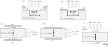
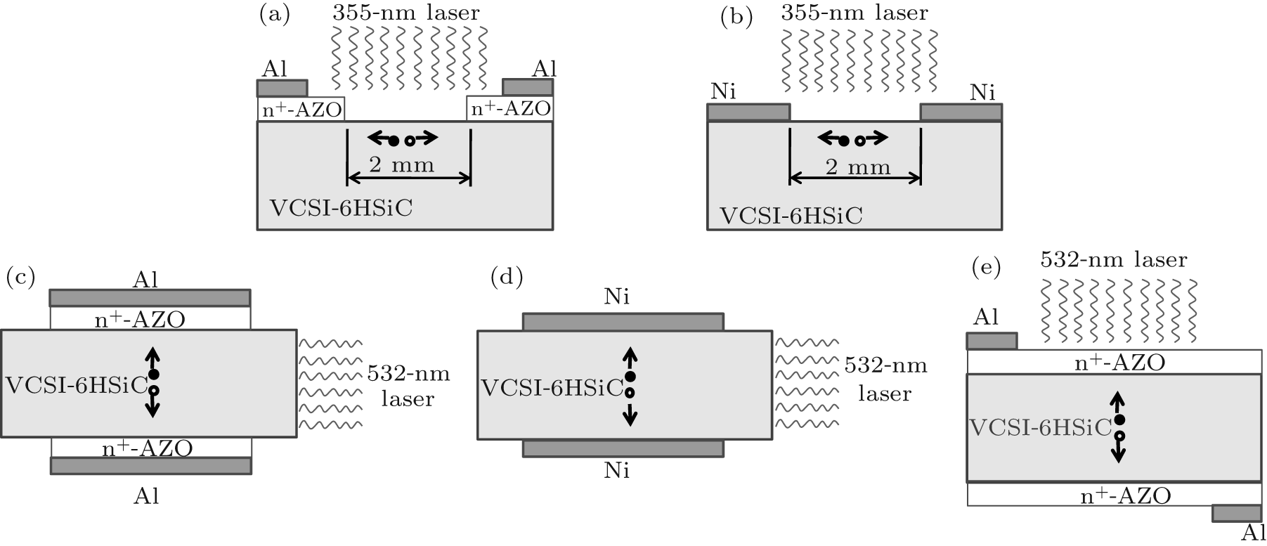
Vanadium-doped semi-insulating 6H– SiC wafers, produced by Shanghai Institute of Ceramics, Chinese Academy of Sciences, were used to fabricate PCSSs in this work. Five devices were fabricated, including two lateral PCSSs and three vertical PCSSs. The two lateral PCSSs were fabricated on c plane 6H– SiC substrates with a thickness of 430 μ m and a size of 1 cm × 1 cm. The three vertical PCSSs were fabricated on a plane 6H– SiC substrates with a thickness of 790 μ m and a size of 1 cm × 1 cm. In the following text and figures, the two lateral PCSS are labeled PCSS-L1 and PCSS-L2, while the three vertical PCSS are labeled PCSS-V1, PCSS-V2, and PCSS-V3. For each kind of PCSS, the quality and electrical properties of the 6H– SiC wafers were measured in order to choose high quality 6H– SiC substrates with the same resistance. Before depositing the contacts, all of the substrates were cleaned by the standard RCA procedure and then dipped into 10% HF acid for 1min to remove the native oxide layer. For PCSS-L1, PCSS-V1, and PCSS-V3, a 200-nm AZO thin film was grown on the 6H– SiC substrate at 400 ° C by radio frequency magnetron sputtering. The patterns of AZO contacts were prepared by the photolithography technique and subsequent acid etching. A 150-nm Al layer was then deposited on the AZO thin film to form an Ohmic contact. For PCSS-L2 and PCSS-V2, only Ni contacts were deposited on the 6H– SiC substrate and then annealed at 1050 ° C for 2 min in Ar by an RTP-500 rapid thermal processor. A schematic diagram of the above five PCSSs is shown in Fig. 2.
Fig. 2. Schematic diagram of lateral and vertical PCSSs: (a) PCSS-L1, (b) PCSS-L2, (c) PCSS-V1, (d) PCSS-V2, (e) PCSS-V3.
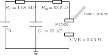
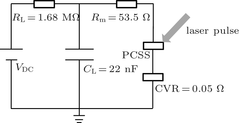
The photoconductivity tests are performed by using 355-nm and 532-nm lasers from a Q-switched Nd:YAG laser with an 8-ns FWHM (full width at half maximum) output pulse for lateral and vertical PCSS, respectively. All of the PCSSs are tested using the same measurement circuit, shown in Fig. 3. A constant resistance of RL = 1.68 MΩ is used to limit large current through the whole circuit and to protect the measurement circuit. The PCSS is charged by a capacitor of CL = 22 nF, which is connected to the high voltage DC power. A load resistance of Rm = 53.5 Ω is used in series with the measured PCSS. A 0.05-Ω current-viewing resistor that has a maximum band width of 1.2 GHz is used to accurately measure the photocurrent signal. A Tektronix DPO4104 digital phosphor oscilloscope with a bandwidth of 1 GHz is used to precisely collect the laser and photocurrent waveforms. According to the schematic circuit in Fig. 3, the on-state resistance Ron of SiC PCSSs is calculated by Eq. (1)
where VPCSS − DC is the applied DC voltage of SiC PCSS and IPCSS is the peak photocurrent through the SiC PCSS at on-state.
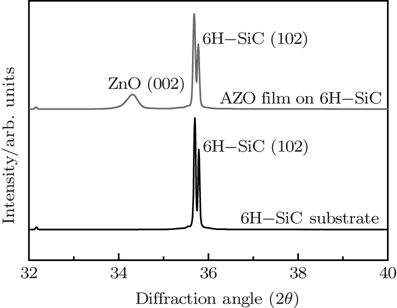
The crystalline quality and electrical property of as-grown AZO thin film were characterized by using the x-ray diffraction (XRD) and Hall effect measurement system. Figure 4 shows the XRD patterns of AZO thin film deposited on c-plane 6H– SiC substrate. A diffraction peak located at 34.3° is clearly seen, which corresponds to wurtzite structure ZnO (Joint Committee for Powder Diffraction Studies (JCPDS), No. 36-1451).[16] The appearance of a ZnO (002) peak indicates the c-axis preferential growth along the c plane of 6H– SiC substrate. The resistivity of AZO thin film measured by the Hall effect measurement system is 3.19 × 10− 3 Ω · cm, and the electron density is 3.92 × 1020 cm− 3.
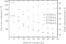
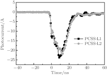
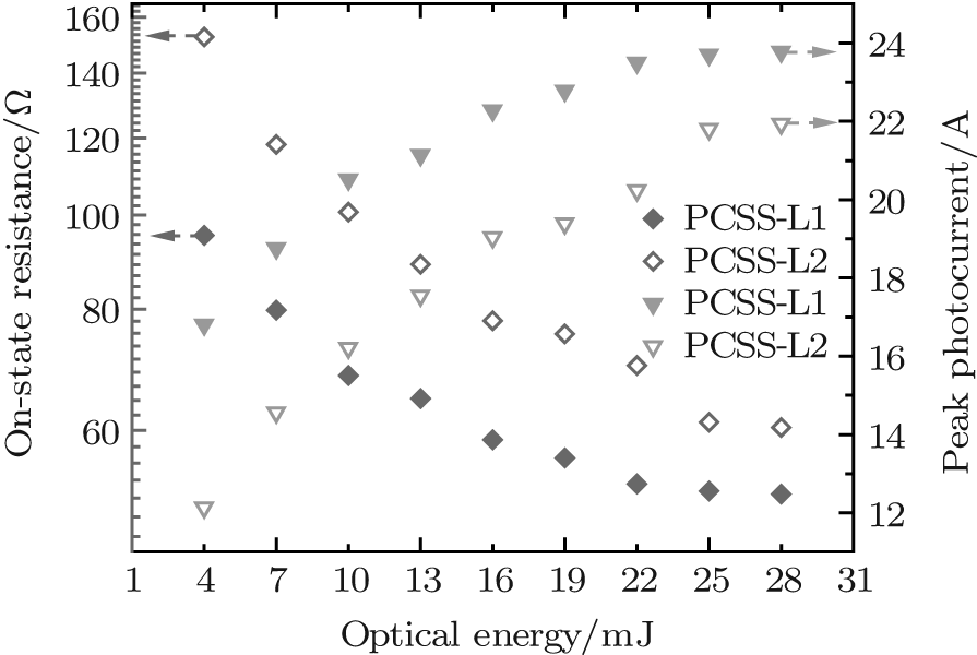
Figure 5 shows the minimum on-state resistance and peak photocurrent of two lateral PCSSs as a function of optical trigger energy from 4 mJ to 28 mJ at 355 nm and 2.5 kV. For PCSS-L1 and PCSS-L2, the on-state resistance rapidly decreases when the optical excitation energy is increased from 4 mJ to 28 mJ. The change trend gradually becomes smooth as the optical trigger energy exceeds 20 mJ, and finally the on-state resistance saturates at above 25 mJ. Note that the on-state resistance of PCSS-L1 is consistently smaller than that of PCSS-L2 from 4 mJ to 28 mJ. When these two PCSSs are triggered at 28 mJ, the on-state resistance of PCSS-L1 is 51.6 Ω , which is 8.9 Ω (14.7% ) smaller than that of PCSS-L2. The dependence of photocurrent on the optical energy shows an exponential increase. The photocurrents of PCSS-L1 and PCSS-L2 start to saturate above 22 mJ and reach maximum values of 23.8 A and 21.9 A at 28 mJ, respectively. The photocurrent waveforms of PCSS-L1 and PCSS-L2 excited at the same saturation conditions are shown in Fig. 6.
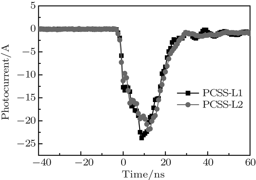
Fig. 6. The photocurrent waveforms of PCSS-L1, PCSS-L2, measured at 2.5 kV and 28 mJ with an excitation wavelength of 355 nm.
Zhu et al. studied the effect of n+ -GaN subcontact layer on the performance of 4H– SiC high-power photoconductive switches. A heavily doped GaN sublayer was epitaxially grown on 4H– SiC substrate by organometallic vapor phase epitaxy (OMVPE).[17] The minimum on-state resistance of PCSS with an n+ -GaN subcontact layer was two orders of magnitude lower than that of PCSS without the GaN subcontact layer. The decrease in minimum on-state resistance was attributed to the heavily doped GaN sublayer, which prevents current crowding, reduces contact resistance and alleviates Joule heating. Heavy doping in the GaN materials can narrow the space charge region of the n+ -GaN/SiC junction and increase the probability of the electron tunneling effect to improve the Ohmic contact property. Since ZnO has the same wurtzite structure as GaN, an n+ -AZO thin film can hold effects similar to those of n+ -GaN. However, the decrease in amplitude of on-state resistance in our study is still much smaller than what Zhu et al. reported. This may be due to a difference in film quality between AZO and GaN. The n+ -GaN thin film on SiC substrate prepared by OMVPE shows monocrystalline characteristics, [18] while the AZO layer deposited by radio frequency magnetron sputtering exhibits polycrystalline behavior. This has been proven by XRD results. There are abundant grain boundaries in polycrystalline thin film, which enhance the scattering effect and collapse the photocurrent. Therefore, it can be deduced that a better quality n+ -AZO thin film will significantly decrease the on-state resistance. Even if a better preparation method is used to prepare AZO thin film, the quality of ZnO may still be a little bit worse than GaN. The lattice mismatch between GaN and 4H– SiC is only 3.5% , which is smaller than that between ZnO and 6H– SiC (5.5% ). The greater compressive stress caused by the higher lattice mismatch reduces the quality of AZO thin film. Table 1 shows the basic parameters of 6H– SiC, 4H– SiC, GaN and ZnO.[19– 21]
Table 1.
Table 1.
Table 1. The lattice parameters of 6H– SiC, 4H– SiC, GaN, and ZnO.
Materials
Lattice constant a, b/nm
Lattice constant c/nm
6H– SiC
a = b = 0.3081
c = 1.5120
4H– SiC
a = b = 0.3081
c = 1.0085
GaN
a = b = 0.3189
c = 0.5185
ZnO
a = b = 0.3249
c = 0.5207
Table 1. The lattice parameters of 6H– SiC, 4H– SiC, GaN, and ZnO.
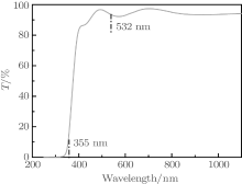
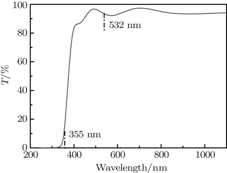
Besides its excellent electrical properties, AZO thin film also has good optical properties that can be used to fabricate opto-electronic devices. Figure 7 shows the transmission spectrum of AZO thin film with a thickness of 200 nm. The AZO thin film was deposited on a quartz glass substrate and measured by using a UV-VIS-NIR spectrophotometer (Cary 5000). It can be seen that the AZO thin film shows a transmission of 11.3% at 355 nm, while it sharply increases to 94.0% at 532 nm. The optical property measurement reveals that a laser light with a wavelength of 355 nm can be strongly absorbed by AZO thin film, while a laser light with a wavelength of 532 nm can almost transmit. The photon energy of 355 nm is larger than the band gap of ZnO (3.4 eV) and can excite a large number of valance electrons to the conduction band. Whereas the photon energy of 532 nm is smaller than the band gap of ZnO, so it can excite only a few impurity levels in the band gap and therefore cannot be absorbed well by AZO thin film.
A laser light with a wavelength of 532 nm is often used to trigger vertical 6H– SiC PCSS at a below-band-gap mode. A large number of carriers from the extrinsic levels in the band gap are excited to the bottom of the conduction band.[22] To make complete use of the n+ -AZO subcontact layer, three vertical PCSSs with different structures were meticulously designed. The structure design is very important for fabricating high performance electronic devices. A different device structure will lead to different performance. Figures 2(c), 2(d), and 2(e) present the different structures of vertical PCSSs corresponding to PCSS-V1, PCSS-V2, and PCSS-V3, respectively. For PCSS-V1 and PCSS-V2, opposite contact structures are used. The only difference is that an n+ -AZO subcontact layer is included in PCSS-V1.
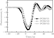
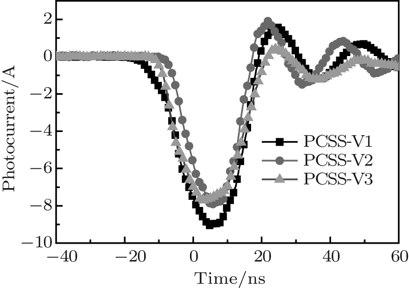
Fig. 8. Photocurrent waveform of PCSS-V1, PCSS-V2, and PCSS-V3 measured at 1.0 kV and 15 mJ with an excitation wavelength of 532 nm.
Figure 8 shows the photocurrent waveforms of PCSS-V1, PCSS-V2, and PCSS-V3, measured at the same conditions. Each photocurrent waveform is obtained statistically using the measurements from a 16-pulse test at 10-Hz repetitive frequency in order to guarantee the data accuracy. It can be seen that the peak photocurrent of PCSS-V1 is 1 A larger than that of PCSS-V2. The corresponding minimum on-state resistance of PCSS-V1 is 57.6 Ω , which is 19.4% lower than that of PCSS-V2 (71.5 Ω ). This further confirms the conclusion that an n+ -AZO subcontact layer can indeed reduce the on-state resistance. It should be noted that there are some disadvantages for the opposite contact structure, even with an n+ -AZO subcontact layer. For instance, the “ surface flashover” that usually occured in lateral PCSS may also take place along the side facet in this structure if the contacts are extremely close to the edge of SiC substrate. This will degrade the hold-off voltage of PCSS. Hettler et al. suggested that a high-dielectric all-encompassing encapsulant is necessary to inhibit surface flashover.[23] However, there are four side facets for this structure. The four side facets cannot be completely encapsulated because one side facet must be unsealed for laser illumination. Thus the opposite contact structure holds an inherent conflict between complete encapsulation and ease of illumination. In addition, laser illumination from the side facet may lead to nonuniform distribution of photocarriers. As the laser intensity gradually attenuates in the 6H– SiC from the illuminated side facet to the opposite side facet, the concentration of photon-generated carriers also decreases gradually. This induces charge crowding near the illuminated side facet, which can significantly degrade the metal contacts when the PCSS is used in an extreme environment. Figure 2(e) shows a diagonal metal contact structure with an n+ -AZO subcontact layer under the Al metal contacts. The obvious characteristic is that the AZO thin film with high transmittance at 532 nm makes direct laser illumination of the substrate from the front facet possible. This novel structure can harmoniously solve the issue of the PCSS with the opposite contact structure. The surface flashover along the side facet can be effectively inhibited due to the entirely closed packaging.[24] Moreover, laser pulse illumination from the front facet can augment the exposed areas and improve the uniformity of photon-generated carrier distribution. All of these assets are beneficial to the thermal stability. However, this diagonal contact structure has a weakness. As shown in Fig. 8, the peak photocurrent of PCSS-V3 is slightly lower than that of PCSS-V2 when measured under the same conditions. This indicates a larger on-state resistance for PCSS-V3, despite the contact resistance being reduced by the n+ -AZO thin film. This may be attributed to a long absorption depth of the 532-nm laser in 6H– SiC (absorption coefficient is 2 cm− 1 at 532 nm[25]), enabling some laser to penetrate directly through the whole PCSS device without being effectively absorbed.
4. Conclusion
An n+ -AZO film is used as a subcontact layer in both lateral and vertical 6H– SiC PCSS to reduce the on-state resistance and optimize the device structure. It is found that heavily doped AZO thin film can improve the ohmic contact property. The on-state resistance of a lateral PCSS with an n+ -AZO subcontact layer is about 14.7% lower than that of a PCSS without an n+ -AZO subcontact layer. Based on the high transparency of AZO film at 532 nm, three vertical PCSSs with different structures are designed, and their performance is discussed. The opposite contact structure of an SiC PCSS with an n+ -AZO subcontact layer presents lower on-state resistance. But the surface flashover induced by incomplete encapsulation may have a negative impact on the hold-off characteristic. Despite the slightly higher on-state resistance, the vertical SiC PCSS with diagonal contact structure facilitates entirely closed encapsulation and favors a uniform distribution of photon-generated carriers, rendering a good trade-off for practical applications.
YuanH, TangX Y, ZhangY M, ZhangY M, SongQ W, YangF and WuH2014Chin. Phys. B23057102DOI:10.1088/1674-1056/23/5/057102[Cited within:1][JCR: 1.148][CJCR: 1.2429]
SullivanJ S and StanleyJ R2006Proceedings of the 27th International Power Modulator Symposium and 2006 High Voltage WorkshopsMay 14–18Washington DC, USApp. 215218[Cited within:1]
23
HettlerC, JamesC and DickensJ2009Proceedings of the 17th IEEE International Pulsed Power ConferenceJune 28–July 2, 2009Washington DC, USA628631[Cited within:1]
WangL N, XunT, YangH W, LiuJ L and ZhangY2014Rev. Sci. Instrum. 85044703DOI:10.1063/1.4870449[Cited within:1][JCR: 1.367]
1
1996
1.438
0.0
... [1#cod#x2013 ...
1
2014
1.148
1.2429
1
2013
1.148
1.2429
... 3] A compact dielectric wall accelerator (DWA) is regarded as one of the most promising applications ...
1
2007
0.0
0.0
... [4] PCSS is considered to be the ideal switch for a compact DWA system due to its lower jitter time, faster response, and smaller volume, compared to a traditional spark gap switch ...
1
1987
0.71
0.0
... [5#cod#x2013 ...
1
1991
0.0
0.0
1
1997
0.0
0.0
... 7] However, despite the rapid progress in Si and GaAs PCSSs, the device performance is strictly limited by the intrinsic material properties, especially at extreme conditions ...
1
2001
1.552
0.0
... [8,9] Thus the Fermi level can be pinned close to the vanadium acceptor level, which results in the semi-insulating nature of vanadium-compensated 6H#cod#x2013 ...
1
1997
1.489
0.0
... [8,9] Thus the Fermi level can be pinned close to the vanadium acceptor level, which results in the semi-insulating nature of vanadium-compensated 6H#cod#x2013 ...
1
2002
0.399
0.0
... [10] Moreover, the inter-band impurities and dopants in vanadium-compensated semi-insulating 6H#cod#x2013 ...
1
2005
0.71
0.0
... [11#cod#x2013 ...
1
1995
3.794
0.0
1
2007
0.0
0.0
... 13] Few studies have focused on concrete ways to optimize the structure and to reduce the on-state resistance of PCSSs ...
1
2010
14.829
0.0
... [14,15] In this paper, an n#cod#x002B ...
1
2014
1.148
1.2429
... [14,15] In this paper, an n#cod#x002B ...
1
2010
1.198
0.293
... [16] The appearance of a ZnO (002) peak indicates the c-axis preferential growth along the c plane of 6H#cod#x2013 ...
1
2005
3.794
0.0
... [17] The minimum on-state resistance of PCSS with an n#cod#x002B ...
1
1996
0.691
0.0
... -GaN thin film on SiC substrate prepared by OMVPE shows monocrystalline characteristics,[18] while the AZO layer deposited by radio frequency magnetron sputtering exhibits polycrystalline behavior ...
1
1998
0.0
0.0
... [19#cod#x2013 ...
1
2009
0.71
0.0
1
2004
1.267
0.0
... 21] ...
1
2006
0.0
0.0
... [22] To make complete use of the n#cod#x002B ...
1
2009
0.0
0.0
... [23] However, there are four side facets for this structure ...
1
2011
0.0
0.0
... [24] Moreover, laser pulse illumination from the front facet can augment the exposed areas and improve the uniformity of photon-generated carrier distribution ...
1
2014
1.367
0.0
... nm[25]), enabling some laser to penetrate directly through the whole PCSS device without being effectively absorbed ...
Application of an Al-doped zinc oxide subcontact layer on vanadium-compensated 6H–SiC photoconductive switches*
[Zhou Tian-Yua),b), Liu Xue-Chaoa)†, Huang Weia), Dai Chong-Chonga),b), Zheng Yan-Qinga), Shi Er-Weia)]


 , Huang Wei