1. IntroductionHigh performance electro-optic (EO) switches are widely used in optical fiber communication systems and optical signal-processing systems.[1, 2] Different materials have been used to fabricate EO switches, including lithium niobate (LiNbO3), gallium arsenide (GaAs), silicon and polymers.[3– 5] However, even for the mature commercial material of LiNbO3, the high switching voltage and the phase mismatch between optical wave and microwave are still obstacles for the future application in wide bandwidth optical communication systems.[6] EO polymers have merits of high linearity, comparatively low dielectric constants for high speed switching, and processing convenience for low cost fabrication. These favorable properties provide them with potential applications in switches, modulators, [7– 9] and other optical devices.[10– 12] For polymer waveguide EO switches with the active layer sandwiched by claddings, the optical loss is crucial for the performance. Much work has been done to design, tailor and optimize nonlinear polymers and chromophores to possess high molecular polarizability from molecular engineering, both theoretically and synthetically.[13– 15] However, extending the light beyond the range of the core layer demands a high performance cladding to lessen the waveguide propagation loss. In fact, a favorable design of a triple-stacked polymer waveguide can provide low loss guidance in selections of core and cladding layer materials. Thus, much work has been conducted to ascertain the influence of mode conditions on the overall device performance.
Besides the physico-chemical compatibility between the claddings and the nonlinear core, which includes the refractive index match to support low loss light signal propagation and the thermal expansion match to obtain smooth film surface, the chemical resistance of the EO core material to the erosion of a solvent in the upper claddings is crucial to the optical loss. These cause high demand for polymers to be used in EO devices.[16– 20] Commonly, thermally curable materials are used in EO switches and plasma etching is adopted to form a rectangular waveguide shape.[7] However, this will inevitably induce physical damage to the core layer, affecting the transmission loss and mode control. Ultraviolet (UV)-curable polymers with high glass transmission temperature (Tg) can provide processing flexibility and physico-chemical compatibility between the core and cladding materials. The application of these UV-curable polymers to an inverted-rib waveguide structure can overcome these defects of a conventional ridge optical waveguide, [21, 22] because photolithographic process and plasma etching are directed at the nature of relative stability of the packet level. Thus, an inverted-rib waveguide configuration is desirable, considering the device fabrication technology and optical loss performance parameters.[23, 24] In addition to these issues, electrodes are also crucial to high-speed optical routing and exchanging applications. Both the device structure and the fabrication technology, such as the optimization of electrode dimensions, should be seriously selected to guarantee the device response performance.[25– 27]
In this paper, UV adhesive of Norland (NOA73) and a guest-host EO polymer of Dispersed Red 1 (DR1) doped UV-curable SU-8 (DR1/SU-8) are used as the passive cladding and active core, respectively. Spectrophotometric analysis, refractive index, and surface morphology characterization are used to study the optical properties of NOA73. The inverted-rib waveguide design is optimized by studying the single-mode operation conditions, characterizations of polarization, and wavelengths dependence. Spin-coating, photolithography, and plasma etching are performed to fabricate a Mach– Zehender (MZ) EO switch with microstrip line (MSL) electrodes. Our measurement results prove the compatibility between UV-curable polymers and nanosecond response time.
2. Inverted-rib waveguide2.1. Active core materialThe optical property of the core material is a crucial issue for the operation voltage and propagation loss of an EO switch. As a low cost, easy-to-synthesized guest-host EO polymer, DR1/SU-8 exhibits an EO coefficient (γ 33) of 15 pm/V after having applied an electric field. Its desirable temperature and time stability are due to the high glass transition temperature (Tg) of 200 ° C and high degradation temperature of 380 ° C of the host polymer SU-8.[28] The refractive index of DR1/SU-8 can be adjusted by varying the UV curing time, thermal treatment temperature, and percentage of DR1 in the mixture.[29] Moreover, DR1/SU-8 shows a good transparency at telecommunication wavelengths with DR1 doping concentration being less than 10 wt%. Thus, it is chosen to be the core material of an inverted-rib waveguide. In this paper, the refractive index of 8-wt% chromophore concentration DR1/SU-8 film is measured to be 1.583, which will be used in the following calculation.
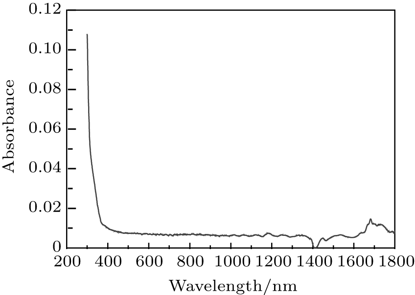
2.2. Passive cladding materialAs mentioned above, the passive cladding plays a key role in realizing the high-performance EO switches. Here, UV-curable epoxy of NOA73 is selected to be the cladding material.[30, 31] It has good adhesion to metal ground electrode (Cr or Au) and can be rapidly UV cured. To confirm its optical properties, the absorbance measurement is carried out by spectrophotometer UV 3600 (SHIMADZU Co., Japan) over a wavelength range of 600 nm– 1800 nm, as shown in Fig. 1. The spectrum proves a low absorption of NOA73 at wavelengths over 400 nm, including wavelengths of 1310 nm and 1550 nm in the near-infrared region. This can lessen the optical loss from an evanescent field, which would be intensified due to a small difference in the refractive index difference between the cladding and core materials.
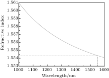
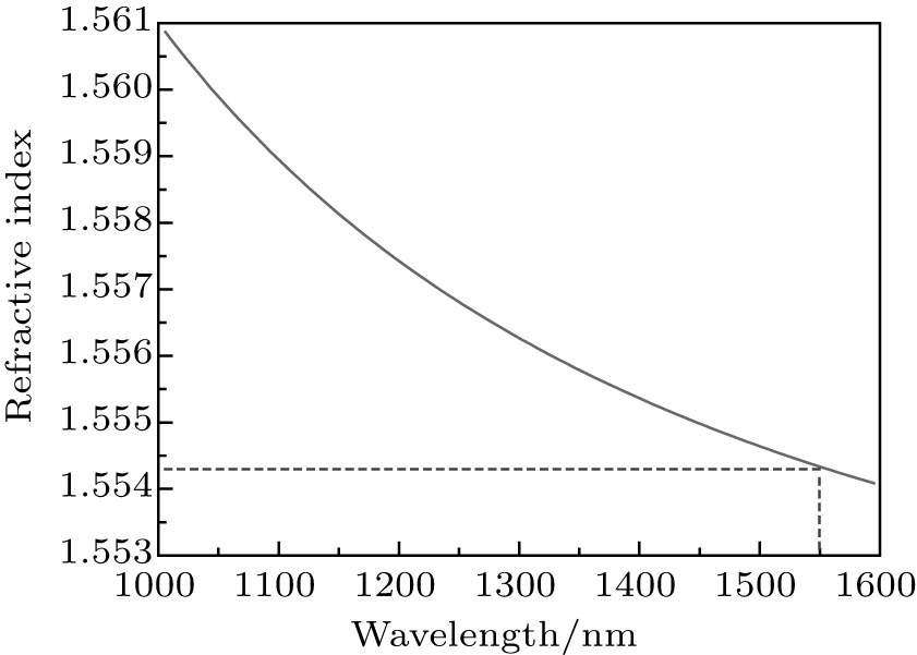
Figure 2 shows the refractive index of NOA73 as a function of wavelength, measured by an ellipsometer M-2000UI (J. A. Woollam Co. Inc., USA) through averaging the measured data of three different samples. At a wavelength of 1550 nm, the refractive index is about 1.5543, which matches with that of DR1/SU-8, facilitating the mode control.
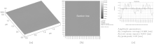
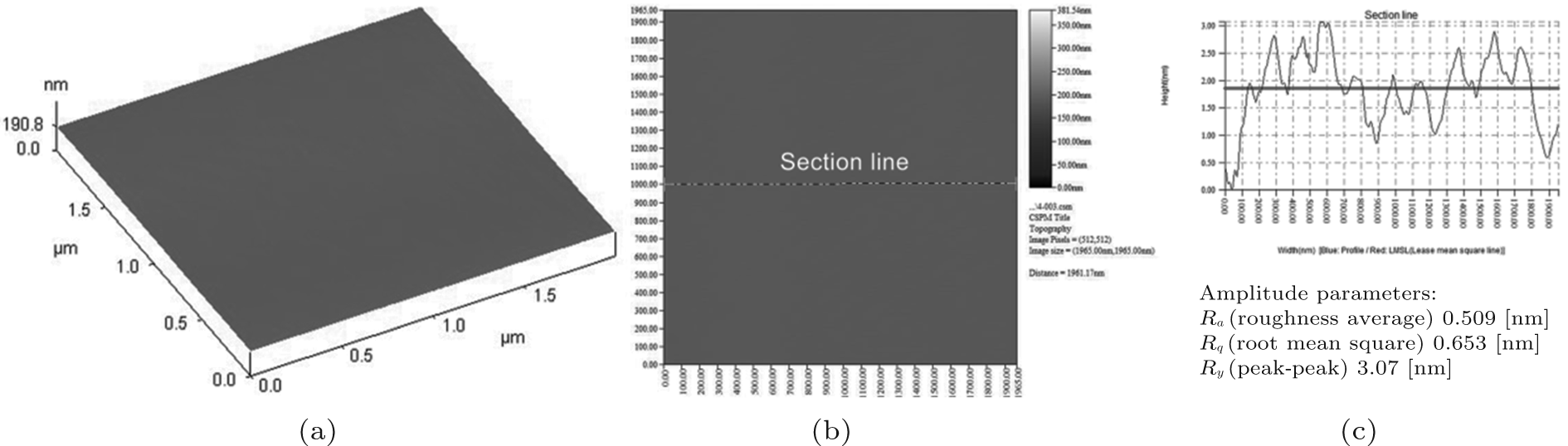
To examine the surface morphology of cladding, the AFM image of NOA73 film is recorded with a multimode scanning probe microscope CSPM5000 (Being Nano-Instrument Ltd., China) that is operated in contact mode, as shown in Fig. 3. The contour-line roughness analysis by characterizing the section line on the planar images in Figs. 3(b) and 3(c) shows that the peak to peak value Ry is 3.07 nm, the average roughness Ra is just 0.509 nm, and the root-mean-square roughness (RMS) Rq is 0.653 nm. In an area of 2 μ m× 2 μ m shown in Fig. 3(a), the RMS roughness is 0.665 nm. Considering the operation wavelength of 1.55 μ m, these results prove a smooth surface that can satisfy the demand for an inverted-rib waveguide cladding to avoid roughness-induced scattering loss.
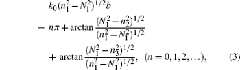
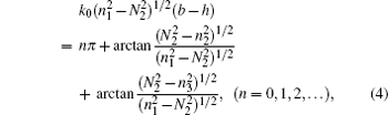
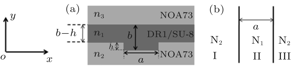
2.3. Design and optimization of inverted-rib waveguideSince higher order modes will seriously degrade the performance of EO switches, a single-mode operation is needed to achieve high extinction ratio and low optical loss. Here, the operation principle and design factors for an inverted-rib waveguide are analyzed according to the single-mode condition, mode size, polarization, and wavelengths dependence. A schematic diagram of inverted-rib waveguide is shown in Fig. 4. The proposed ridge waveguide design is built on the concept modification of Fischbeck et al., [32] and has already been applied to inorganic waveguide devices.[33] In this study, a groove with specified width and depth is firstly introduced on the surface of NOA73 lower cladding. Then, DR1/SU-8 is spin-coated as the core layer, forming an inverted-rib structure.
According to what Fischbeck et al. reported in Ref. [32], the single-mode operation condition in this design can be described as

where a and b are the width and thickness of the ridge waveguide, respectively, and h is defined as the height of ridge. It should be pointed out that this equation works only on condition that

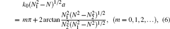
As shown in Fig. 4(a), n1 is the refractive index of DR1/SU-8, n2 and n3 are the refractive indices of the upper cladding and lower cladding, respectively. Based on the effective index method (EIM), eigenvalue equations on  in the equivalent slab waveguide can be expressed as
where

N1, N2, and N3 are the effective refractive indices in regions of I, II, and III, respectively, and λ is the optical wavelength.[34] Therefore, the effective refractive index Neff for  and
and  modes can be calculated, respectively, from the following equations:

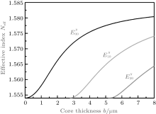
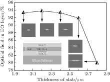
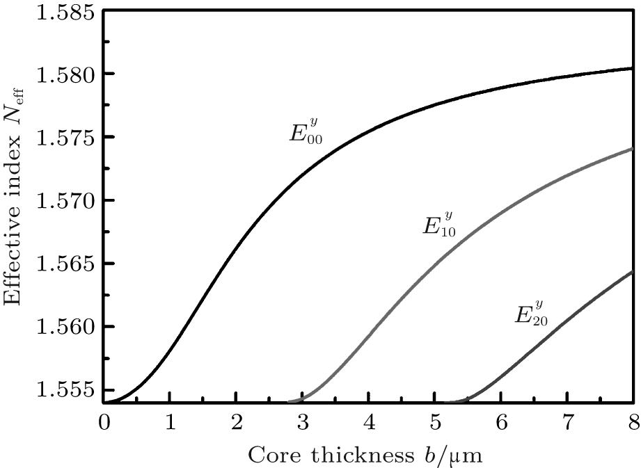
The relations between the core thickness b and the effective refractive index Neff of the inverted-rib waveguide are calculated, as shown in Fig. 5, where a is chosen to be 1.5b. The maximum thickness of the DR1/SU-8 layer is determined from the condition that  mode begins to appear or cut out. Thus, b should be chosen to be within 3 μ m to realize single-mode propagation of
  mode in the inverted-rib waveguide. In fact, the thickness of core layer is chosen to be as large as possible with maintaining a single propagating mode to enlarge the optical intensity in core layer, thereby reducing the optical loss when coupling with fibers. Though radiation modes and weakly confined modes may be excited by increasing the thickness of the core layer, they can be eliminated by the absorption from metal electrodes through appropriately selecting the cladding material and its thickness.
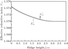
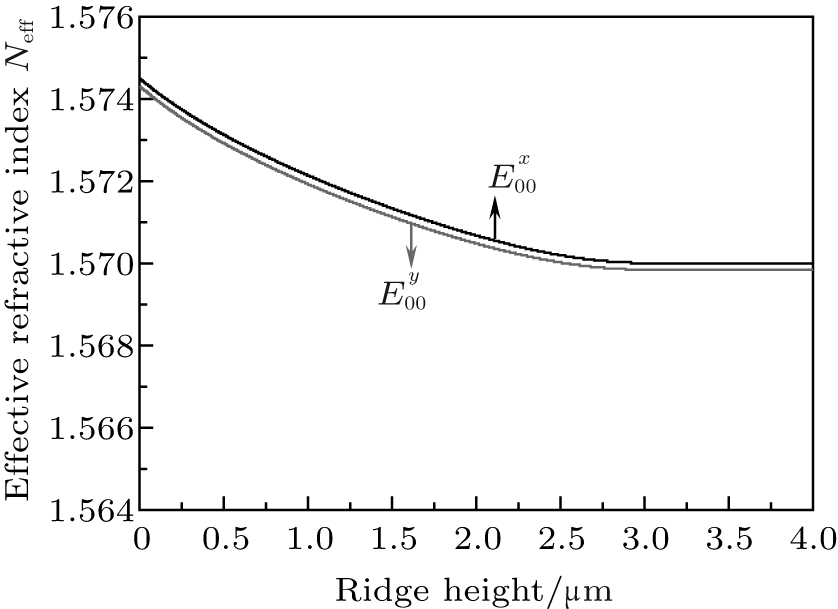
As shown in Fig. 6, when the ridge height increases from 0 to 1 μ m, the effective refractive indices of  and
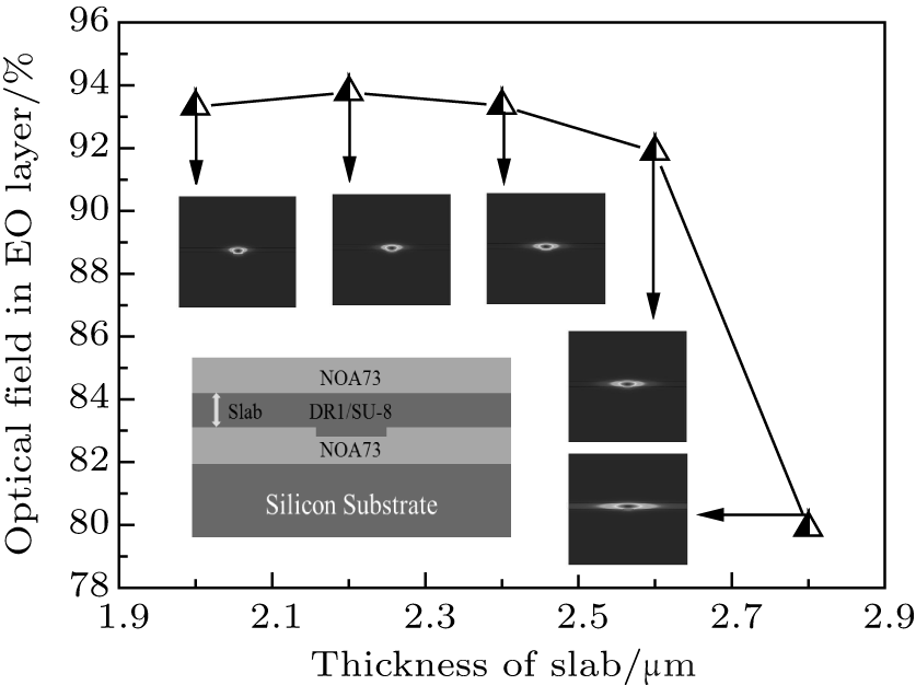
and  modes monotonically decrease from 1.5743 and 1.5745 to 1.5719 and 1.5721, respectively, with other parameters fixed. An optimized ridge height is assumed to be within the single-mode range far from the cutoff, ensuring that the mode is strongly guided. Therefore, field distributions of the fundamental mode with different ridge heights are computed, which are shown in Fig. 7. It can be seen that with h increasing from 0.2 μ m to 0.8 μ m, the percentage of optical field distributed in the core layer in comparison with the total optical field distributed in the cross-sectional area of the inverted waveguide increases from 79.91% to 93.78%. However, the percentage begins falling as h is larger than 0.8 μ m. Thus, the ridge height is chosen to be 0.8 μ m to enhance the field intensity in the core layer.
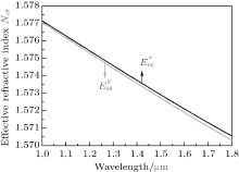
Figure 8 shows the effective refractive index change of fundamental modes of  and
and  when the optical wavelength increases from 1.0 μ m to 1.8 μ m in steps of 0.1 nm (i.e., Δ λ = 0.1 nm) on condition that other parameters are fixed. It shows that Neff of
  mode is always smaller than that of
  mode. Both modes monotonically decrease with the increasing of wavelength. At 1550 nm, the difference in effective refractive index between
  and
and  modes is less than 2.3× 10− 4, which proves the polarization insensitivity of this inverted-rib waveguide.
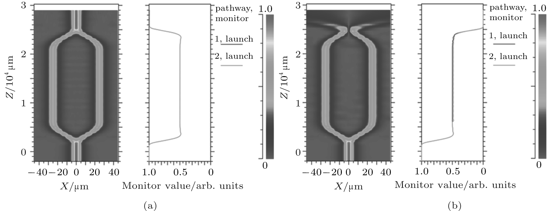
The light propagation of the MZ-type EO switch with micro-strip line electrode is computed by the beam propagation method, as shown in Fig. 9. A driving voltage is applied to present the switching performance in the calculation. No phase mismatch exists between the two arms of MZ switch when no voltage is applied. The output shows the maximum optical power, which corresponds to the “ on” state. When a switching voltage is applied to one arm, the EO effect results in a phase difference of π between the two arms and thus the switch output is minimum, which corresponds to the “ off” state.
In general, the inverted-rib structure can provide a larger single-mode cross section with specified dimensions and the distinct difference in refractive index between the core and cladding materials is compared with that in the common rectangular waveguide concept. Moreover, the groove defined on the robust UV-cured NOA73 cladding lessens the plasma etching induced sidewall roughness and the consequent scattering loss.
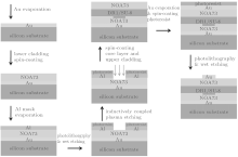
3. Device fabrication3.1. EO polymer preparationThe widely used UV-curable polymer SU-8 2005 (MicroChem Corp.) is doped with DR1 and thoroughly stirred to guarantee full mixing. The high absorption of chromophores in the UV region causes chemical cross-linking of SU-8 to happen.[29] To enhance the above process and reduce the relaxation of chromophores, 3.5-wt% triarylsulfonium salt photoinitiator is introduced into DR1/SU-8.
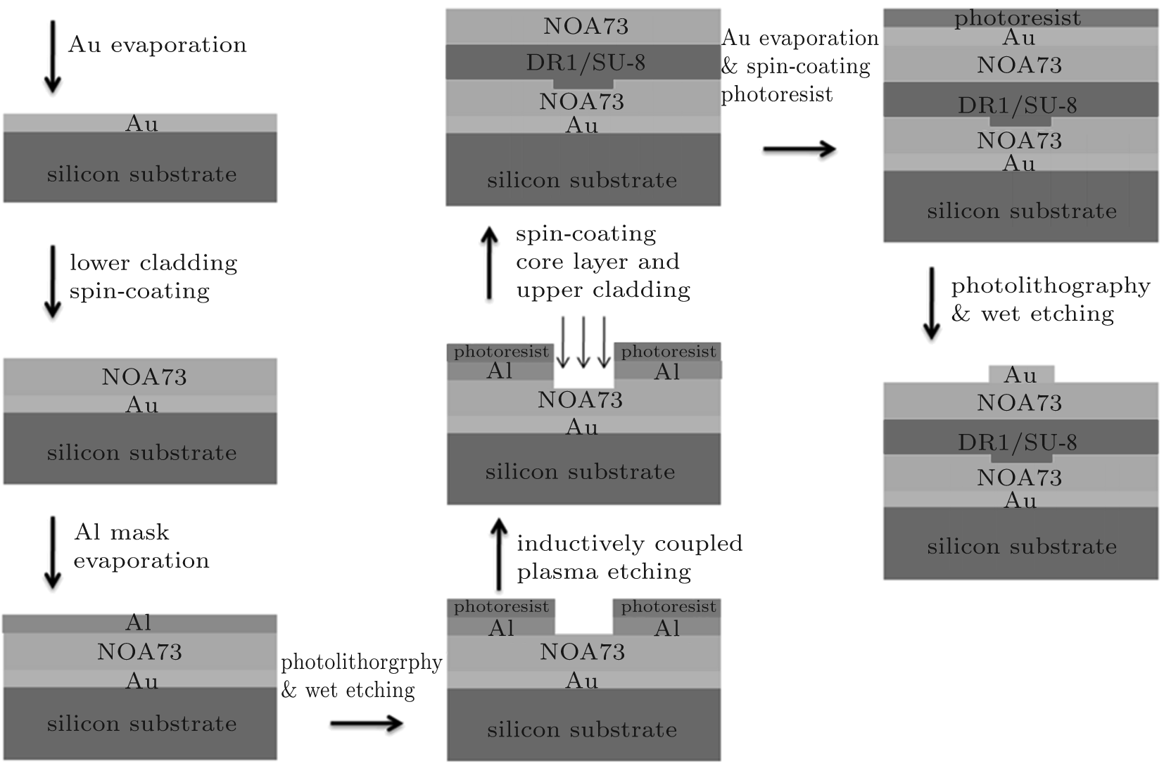
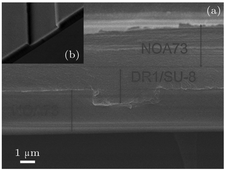
3.2. Waveguide fabricationA schematic diagram of fabrication process is presented in Fig. 10. Firstly, the thermal evaporation method is used to deposit high-purity (> 99.999%) solid Au thin metal film with a thickness of 0.5 μ m on the silicon substrate that is to be used as the ground electrode. After that, the solvent-free UV-curable polymer NOA73 is spin-coated at 5000 rpm, yielding a 3.5-μ m thick film. It is then exposed under a mercury lamp (Newport Co., 10 mW/cm2 at 365 nm) for 140 s and post-exposure baked at 120 ° C for 2 h to enhance cross-linking. After that, a layer of 100-nm-thick aluminum film is thermally evaporated onto NOA73 film as a metal mask. To define waveguide patterns on the aluminum film, BP212 photoresist is spin-coated and patterned by traditional photolithography (ABM Co. Inc, U.S.).[35] The inductively coupled plasma etching process in O2, SF6, and CF4 atmospheres is performed for 110 s in a 13.56 MHz CE-300I (ULVAC Co. Inc, Japan) etching machine to form a groove with a depth of 0.8 μ m on NOA73 surface.[36] The DR1/SU-8 film with a thickness of 3 μ m is formed by spin-coating process on NOA73 cladding. Then, the sample is pre-baked at 65 ° C for 10 min and 90 ° C for 20 min to remove the residual solvent. After that, it is UV cured by the same mercury lamp for 180 s, followed by a post-exposure baking at 95 ° C for 15 min and 135 ° C for 1 h to enhance the cross-linking of EO polymer. The upper NOA73 cladding is spin-coated and cured. Finally, the upper electrode is formed by thermal evaporation, photolithography, and wet chemical etching. Figure 11 shows a scanning electron microscope (SEM) image of the interface morphology and the cross-sectional view of inverted-rib waveguide. No evidence for solvent erosion or dissolution is observed at the interface between DR1/SU-8 core layer and NOA73 cladding, which is favorable to stabilizing the alignment of chromophores in SU-8. As shown in the inset of Fig. 11, the vertical profile, flat bottom, and smooth side-walls of NOA73 groove will lessen the scattering loss, and the consequent propagation loss as well. Before performance measurement, the waveguide sample is sliced by a wafer dicing machine DAD-3220 (DISCO Co. Inc, Japan).
3.3. Electric polingTo avoid the passive effects that are induced by UV light and high temperature treatment on the alignment of chromophores, [37] parallel plate electric field poling is used to preferentially align DR1 chromophores and induce a nonzero EO coefficient γ 33.[38] After that, the upper poling electrode is also used as the modulation electrode. Since no further heating process is applied after poling, it is favorable to the optical nonlinearity stability of the EO polymer and the performance of the EO switch. Here, a poling voltage of 800 V is applied to the three layer stacks in 25 V steps per 0.1 min at room temperature. After that, the sample is heated to 200 ° C at a rate of 10 ° C/min to avoid decomposing the chromophores. Considering the resistivity values of 3.5× 10¹¹ Ω · cm and 9.5× 10¹¹ Ω · cm for NOA73 and DR1/SU-8 at 200 ° C, respectively, a field about 143 V/μ m (430 V) is applied to the EO layer based on the equivalent electrical circuit for direct-current electric poling.[37– 39] After 30 min, the sample is gradually cooled to room temperature. The whole process is carried out in a N2 atmosphere to prevent poling-induced optical loss.
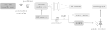
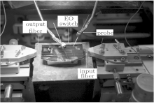
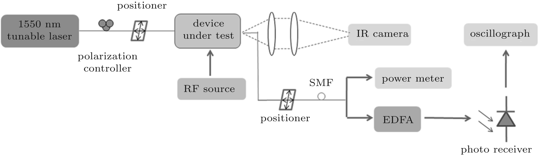
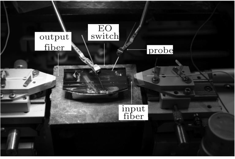
4. Results and discussionThe time response and insertion loss of the switch are evaluated by the testing system shown in Fig. 12. Light with a wavelength of 1550 nm from a tunable laser TSL-210 (Santec Co., Japan) is perpendicularly polarized to the waveguide plane by passing through a polarization controller and butt-coupled into the waveguide. The output fiber alignment is optimized with a five-axis position control to maximize the optical output of the switch, as is the input fiber alignment, until the best condition is achieved. A standard single-mode fiber is used to couple the output signal to an optical power meter AQ8203 (Ando Electric. Co. Ltd., Japan) to measure the optical insertion loss. The far-field light output is monitored by an infrared (IR) charge-coupled device camera with 200 magnification. The rectangular modulating signal from generator SP1461 (Sample Instrument Co. Ltd., China) is fed into the MSL electrode through microprobes. The modulated optical signal is converted into an electrical signal by a photodiode GT322D (CETG Co., China). The electrical signal is observed on an oscilloscope DPO 4104B (Tektronix Inc., USA). Figure 13 shows a photograph of the EO switch under test.
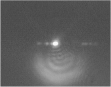
Figure 14 shows the far-field light output from the MZ switch at 1550 nm. No significant slab-induced light spreading is observed. The measured optical insertion loss of a 3-cm-long MZ interferometer switch is about 12.5 dB, which includes a coupling loss of 5 dB (2.5 dB/fact) that is induced by mode mismatch, air gap, and roughness of the input and output waveguide facets, propagation loss of about 7.5 dB induced by an absorption loss of 2 dB/cm from DR1/SU-8 (1.5 dB/cm) and NOA73 (0.5 dB/cm). Besides, Y branch couplers, imperfect sidewall roughness, and slant configuration of waveguide caused by photolithography and ICP etching process lead to a scattering loss of 0.5 dB/cm.[40, 41] Thus, the propagation loss of the switch is about 2.5 dB/cm.
These results are based on the fact that several issues, including material absorptions, birefringence, refractive index match, waveguide configuration, mode dispersion, roughness, and inhomogeneity, may affect optical loss. Since there is such a huge mismatch in the respective attenuation, it is not obvious that the loss is due to one single cause. Therefore, optical loss can be improved from both technical and scientific aspects. In this paper, the attenuation for an optical waveguide is largely attributed to scattering due to the presence of imperfections in the core-cladding interface or in the core itself. Commonly, the vertical surfaces or sidewalls of polymer waveguides are created by etching. Their smoothness relies on the quality of the mask used during the photolithography process. A rough mask will produce rough walls as the etching reproduces the mask imperfection with a great fidelity.[42, 43] Therefore, a precise mask is crucial for photolithography to achieve a smooth sidewall, and scattering loss can be reduced effectively through studying the effect of sidewalls scattering due to surface roughness and sidewall roughness.[44, 45] Moreover, high-quality waveguide sidewalls can be obtained by different fabrication methods, such as soft molding processes by UV embossing through a facile UV photopolymerization under the ambient conditions on various substrates.[46] Wet etching that avoids bombarding the plasma is also fit for achieving smooth sidewalls to restrain scattering in the waveguide.
The reason why a long modulation arm is adopted in this paper is due mainly to the optimization of the switching voltage. When a π phase difference is generated between the two branches of an MZ-type EO switch with an MSL electrode, the corresponding half-wave modulation voltage Vπ can expressed as
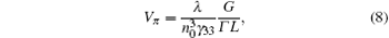
where λ is the communication wavelength, n0 is the refractive index of the EO material.[8] It can be seen that Vπ is determined mainly by modulation length L, gap between voltage electrodes G, EO coefficient γ 33, and EO overlap integration factor Γ . n0 and γ 33 are determined by waveguide configuration and poling efficiency. Given the fixed material and MSL electrode characteristics, Vπ can be reduced effectively through increasing the modulation length L. Because of this, a compromised 1.5-cm long modulation length is adopted in this paper. However, the length of EO switch can be reduced by nearly 40%, according to the requirements of application and integration. Besides, if a ring resonator structure is adopted, the modulation length and then the size of switch can be effectively diminished.[27, 47– 49]
Here, an MSL electrode instead of co-planar waveguide (CPW) electrode is used to enhance the EO overlap integration factor Γ . According to the following equation:
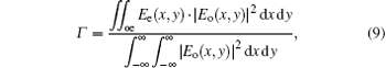
Γ corresponds to the signal electric field distribution in an optical waveguide layers normalized to the field that will appear if air is the dielectric.
Here, Ee(x, y) and Eo(x, y) are the external electric field and mode optical field distribution over the waveguide cross-section, respectively. For the operation mode of this switch, it is clear that an effective operating electric field should be applied to the direction in which DR1/SU-8 has been poled. Therefore, only the alignment vector component in the direction perpendicular to DR1/SU-8 film surface has contributions to EO modulation. The alignment vector component in the horizontal direction has no contribution to EO modulation. Through the investigation of electric field distributions generated by MSL and CPW electrodes across the polymer waveguide, switches with MSL electrode will result in a higher EO overlap integral Γ than with adopting CPW electrode, which is in favor of the switching voltage.[8] According to our calculation, Γ will increase from 47.43% to 89.52% when adopting the MSL electrode instead of the CPW electrode. Besides, the dielectric characteristic of substrate has more remarkable effects on the bandwidth performance for a device that adopts a CPW electrode. Thus, an MSL electrode is adopted in this switch.
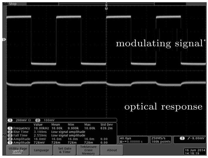
The time response is measured and presented in Fig. 15, where the rectangular driving signal at 10 kHz and the detected optical response are both simultaneously illustrated as the upper and lower waves, respectively. The rise time and fall time of switching are 3.199 ns and 2.559 ns, respectively. This nanosecond response proves the effectiveness of an EO switch that adopts an inverted-rib structure and UV-curable polymers as waveguide materials. In fact, the switching speed mainly depends on the RC characteristic of the waveguide. In this design, the width and length of the upper electrode in a modulation region are 20 μ m and 15 mm, respectively, which corresponds to an area of 0.3 mm2. Considering the low dielectric constants of about 4 for NOA73 and SU-8 polymers, the switch would exhibit better performance in a case where the dimension of the electrode is reduced and optimized.
The switch exhibits only an extinction ratio of less than 6 dB at the best level. This result originates from the fact that the change of optical output intensity is determined mainly by the EO coefficient γ 33 and EO overlap integration factor Γ , which can be optimized by waveguide and electrode design. For fixed configuration design and modulating voltage, γ 33 will affect the extinction ratio remarkably. The on-chip EO coefficient of poled DR1/SU-8 is just around 7.5 pm/V compared with that of high performance nonlinear polymers. Therefore, the intensity change is seriously limited by the nonlinearity of DR1/SU-8.
Except for the material properties, the orientation relaxation of nonlinear molecules and poling efficiency have an evident effect on the extinction ratio. As has been mentioned before, contact poling is adopted to align DR1 chromophores in this paper. Although a higher poling voltage can be adopted theoretically, we find that the inevitable nonuniformity and defects on film surface due to fabrication will lead to dielectric breakdown at a high voltage. Therefore, the poling voltage cannot be improved unboundedly, and DR1 chromophores will not be aligned completely, which results in a low EO coefficient. Cladding materials either with significantly lower relative permeabilities or significantly higher dielectric constants than those of the core material will be adopted to maximize the voltage dropped across the core layer, which is favorable to enhancing the modulation depth and extinction ratio.


 , Chen Chang-Ming