Light trapping characteristics of glass substrate with hemisphere pit arrays in thin film Si solar cells*
[Chen Lea), b) , Wang Qing-Kanga)†  , Wangyang Pei-Hua
a) , Huang Kuna) , Shen Xiang-Qiana) ]
, Wangyang Pei-Hua|
|


†Corresponding author. E-mail: wangqingkang@sjtu.edu.cn
*Project supported by the National High-Tech Research and Development Program of China (Grant No. 2011AA050518).
In this paper, the light trapping characteristics of glass substrate with hemisphere pit (HP) arrays in thin film Si solar cells are theoretically studied via a numerical approach. It is found that the HP glass substrate has good antireflection properties. Its surface reflectance can be reduced by ∼ 50% compared with planar glass. The HP arrays can make the unabsorbed light return to the absorbing layer of solar cells, and the ratio of second absorption approximately equals 30%. Thus, the glass substrate with the hemisphere pit arrays (HP glass) can effectively reduce the total reflectivity of a solar cell from 20% to 13%. The HP glass can also prolong the optical path length. The numerical results show that the total optical path length of the thin film Si solar cell covered with the HP glass increases from 2 ω to 4 ω. These results are basically consistent with the experimental results.
Thin film silicon cells are an important class of photovoltaics that are currently the subject of intense research.[1– 6] Compared with traditional crystalline silicon (c-Si) solar cells, thin film silicon solar cells have great advantages, such as low cost, easy process, and saving material.[7] Many thin film Si solar cells have been demonstrated, including single-junction hydrogenated amorphous silicon (a-Si), [4] tandem-junction amorphous/microcrystalline silicon, [8] and triple-junction amorphous silicon.[9, 10] However, the thickness of the absorber layer for thin film silicon solar cells is only about hundreds or thousands of nanometers, which is not sufficient to absorb long wavelength light for solar spectrum.[11] Therefore, the power conversion efficiency (PCE) of thin film Si solar cells is relatively low compared with those of crystalline silicon and polycrystalline Si solar cells.[12] In order to improve the PCE of thin film silicon solar cells, many light trapping techniques have been adopted to enhance the light absorption by the optimized optical structure, such as nanowire, [13] nanohole, [14, 15] nanorod, [16] and nanocone.[17, 18] Generally, for thin film silicon solar cells, there are two typical methods to modify the light trapping structure. One is to use the random texture which can provide very reflective light trapping; the other is to add the external optical elements which can make more escaped light come back into the solar cell.[12– 18]
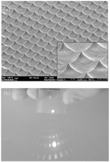
Although conventional light trapping structures can increase the optical path length inside solar cells and result in enhancing light absorption significantly, the drawbacks of these light trapping structures are always in the size range of tens to hundreds of nanometers. Moreover, these nanoscale structures are insensitive to the light of the long-wave band, and the fabrication processes of these nanostructures are relatively complex and expensive, [19, 20] so they are unsuitable for large scale applications for solar cells. In order to overcome these drawbacks, a larger scale light trapping structure was fabricated on the incident side of an optical quartz glass by our research group as shown in Fig. 1(a). It is a periodic micro-hemispherical pit (HP) arrays, the periodic and the diameter of the pit are about 10 μ m and 4 μ m– 5 μ m, respectively.[21, 22] Compared with conventional nanoscale light trapping structures, this glass with micro-HP arrays (HP glass for short) is not only cheap and easy to fabricate, but also very sensitive to the long-wave band. The fabrication of the HP glass consists mainly of only three processes: (i) sputtering, (ii) ultraviolet (UV) lithographing, and (iii) wet etching. Not only can the HP glass effectively reduce the surface reflectivity, but also diffract and scatter the incident light well as shown in Fig. 1(b); therefore, it can significantly enhance the PCE of thin film Si solar cells. Our test results showed that the short circuit current density and total PCE can each be increased about 8% and 5% by covering the HP glass on the surface of thin Si film solar cells.[21]
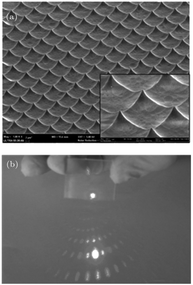 | Fig. 1. (a) The scanning electron microscope (SEM) image of the HP arrays, the magnified image is inserted on the bottom right corner. (b) The diffraction patterns of a laser beam (650 nm) passing through the HP glass. |
These experiment results have demonstrated that the HP glass substrate can effectively enhance the light absorption, but the mechanism research of light absorption increase on this HP glass, especially the light trapping characteristics in thin film Si solar cells, is lacking. Moreover, little theoretical research on the light trapping glass substrate for photovoltaic devices was reported. Therefore, a numerical analysis approach is used to study the light trapping characteristics of the HP glass in this paper, including antireflection properties, total reflectivity, and total optical path length.
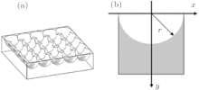
The model of the HP array glass is shown in Fig. 2(a), and the cross section of the hemisphere pit is shown in Fig. 2(b). The cross section can be reduced to an equation of a circle in a simple form, as shown in the following:

where r is the radius of the hemisphere pit. For convenience, it can be set to be a constant 1, so equation (1) can be expressed as

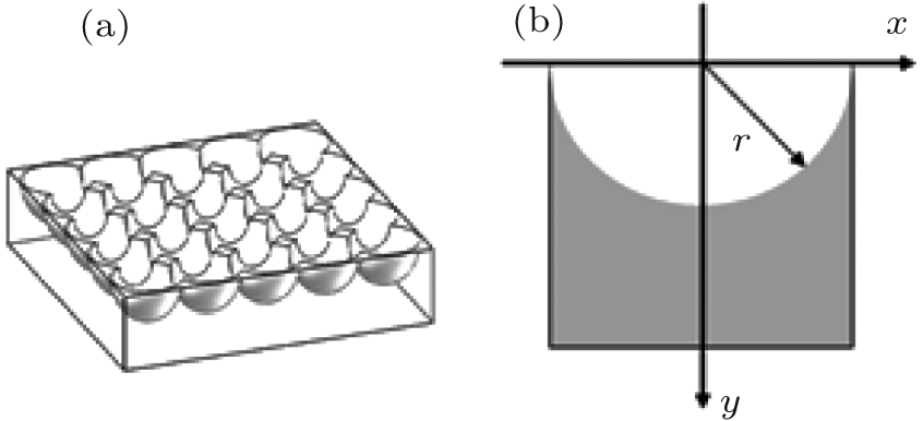 | Fig. 2. (a) Three-dimensional stereogram of the HP glass. (b) The mathematical model of two-dimensional cross section about the hemisphere pit. |
When the size of light trapping structure is far smaller than the wavelength of incident light, we can neglect the influence of structure and take its surface as a smooth plane, the reflection effect on the incident light will be dominant. When the size of structure is considerably larger than the wavelength of incident light, the diffuse reflection will occur. However, when the size of structure is comparable to the wavelength of incident light, the diffuse reflection and specular reflection will occur.[23] In fact, the effective absorbance range is from 0.3 μ m to 1.1 μ m for thin film Si solar cells, and the response sensitivity is dependent on the incident light wavelength.[24] So, the diffuse reflection will occur on the surface of HP arrays, because the size of the hemispherical pit is 10 μ m, which is considerably greater than the response wavelength of the solar cell. Because the radii of these pits are all much greater than the wavelength of incident light, we can ignore the wave nature of light. For smaller radius of the pit, the wave nature of light, such as the diffraction effect, should be taken into account, but we should develop a smaller scale lithography mask, which will be used in the fabrication of the HP glass substrate. Unfortunately, this can lead to spending more on manufacturing. Second, it will affect the light trapping characteristics of the glass if the radius of the pit is approximately equal to the wavelength of incident light, and this will make the problem more complicated. Thus, the analysis method of this paper is not suitable when the radius of pit is very small. Therefore, only the radius of pit which is larger than the wavelength of incident light is considered in this paper.
According to the cross section equation of the HP arrays, the incident light will be averagely divided into many tiny light beams. Based on the geometrical optics theory, the light trapping characteristics of glass substrate with hemisphere pit arrays for thin film Si solar cell application are discussed below.
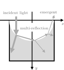
When a beam of light falls on the surface of the hemisphere pit, it will produce multiple reflections as shown in Fig. 3. The intensity ratio of reflected light to incident light is defined as the reflection coefficient, which is a function relating to the refractive index of material, and the incident angle and polarization of light.
 | Fig. 3. Multi-reflection schematic diagram of a light beam in a hemisphere pit structure. |
For the TE polarized light, the reflection coefficient is defined as
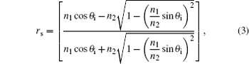
where n1 and n2 are the refractive indices of air and glass, respectively, and θ i is the incident angle.
For the TM polarized light, the reflection coefficient is defined as
For unpolarized light, reflection coefficient r is the average of rs and rp, i.e.,

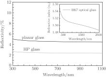
Only the unpolarized light is considered in this paper, and n1 = 1 for air, n2 is a function of the wavelength of incident light for real glass (as shown in Fig. 4).[25] So for the HP glass, the surface reflection ratio (reflectivity) to the incident light is expressed as follows:

where r is the reflection coefficient, j is the number of tiny light beams, and k is the number of reflections for each tiny light beam in the hemisphere pit. For different tiny light beams, the values of k are different; however, for planar glass, when θ i = 90° , the surface reflectivity can be expressed as follows:

Figure 4 shows the surface reflectivities of the planar glass and HP glass, which are obtained from the above equations. It shows that the surface reflectivity of the HP glass can be dramatically reduced by approximately a half compared with that of the planar glass. The decreasing of the surface reflectivity means the increasing of the transmittance of light, so the transmittance of the HP glass wafer increases 2%– 3%, which is consistent with our previous experimental result.[19]
 | Fig. 4. Variations of surface reflectivity with the wavelength of planar glass and HP glass. The relation between the refractive index of BK7 optical glass and the wavlength of incident light is shown in the inset. |
When the light passes through the glass and irradiates at the absorbing layer of a cell, it will be reflected to air or absorbed by the absorbing layer of the cell. The more the reflective light (unabsorbed light), the more easily the efficiency of the cells decreases. Conversely, the efficiency of the cell will be increased. An important function of the HP glass is that it can make the unabsorbed light return to the absorbing layer. To calculate the probability with which the light is reflected back by the bottom of the glass, the method of ray tracking is adopted.
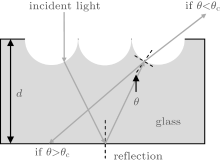
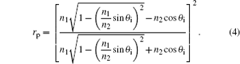
Figure 5 shows the schematic diagram of light in the HP glass on the assumption that all the beams of light will produce total reflection at the bottom of the HP glass. When the light goes from glass into air, the light will leave the glass if θ < θ c, otherwise it will be reflected back to the absorbing layer of the cell. This process continues until the light leaves the glass. The θ and θ c above are the incident angle and the critical angle of light, respectively, and θ c can be obtained from Snell’ s law:

where n1 and n2 are the refractive indices of air and glass, respectively. When we choose the refractive indices n1 = 1 and n2 = 1.5, the critical angle is θ c = 41° .
 | Fig. 5. Schematic diagram of the light in HP glass. |
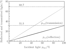
As mentioned above, the incident light is averagely divided into many tiny light beams, and then the tiny light beams are released one by one; in the meantime, supposing that all of the tiny light beams are completely reflected by the bottom glass substrate according to the law of Snell. Based on the above algorithm, the propagation path of each tiny beam can be obtained. Shown in Fig. 6 are the numerical relationships among the numbers of the incident, transmitted, and reflected light beams, with ptra (Ntra/Nall)× 100%, pref = (Nref/Nall) × 100%, and pinc = (Ninc/Nall) × 100% denoting the percentages of transmitted light, the reflected light, and the incident light from the total incident light, respectively, and with Nall, Ninc, Nref, and Ntra representing the numbers of all the tiny light beams, the incident light beams, the reflected light beams, and the transmitted light beams. The ptra, pref, and pinc are related by pinc = ptra ± pref. ptra and pref would make a linear increase pinc. When pinc = 100% and ptra = 68.7%, then pref = 31.3% . The result means that the HP glass is able to make some unabsorbed light beams return to the absorbing layer and make the second absorption. The percentages of the second absorption light and the transmission light are 31.3% and 68.7%, respectively.
 | Fig. 6. Numerical relationships among ptra, pref, and pinc. |
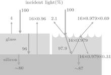
To arrive at the absorbing layer of cells, the incident light must pass through the surface glass. So before arriving at the absorbing layer, multiple reflections and refractions of light will occur. The HP glass has a very good anti-reflective ability. It can make the total reflectance of light decrease greatly in cells, and the absorption of light and the efficiency of the cell increase. For convenience, we also choose the refractive indices of air, glass, and silicon to be n1 = 1, n2 = 1.5, and n3 = 3.5, respectively.[26] We can obtain the reflectivities of light among each layer of air, planar glass or HP glass and silicon as shown in Fig. 7.
 | Fig. 7. Reflectivities of light among the layers of air, glass, and silicon. The left side is a planar glass substrate, and the right is an HP glass substrate. |
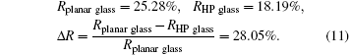
Based on the distribution of light intensity in Fig. 7, the good anti-reflection (AR) performance of the HP glass is clearly shown by comparing with the planar glass. The reflectivities of the planar glass and HP glass could be quantitatively characterized by the following equations:

where Rplanar glass and Rplanar glass denote the total reflectivities of light of the planar glass and the HP glass, respectively, and Δ R represents the relative reduction of the total reflectivity of light. This result shows that the HP glass can effectively reduce the total reflectivity of light in the cells from 20% to 13%, and the relative reduction of total reflectivity goes up to 35% as compared with the reflectivity of the planar glass.
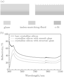
In order to prove these numerically computed results, we conduct the following experiments as shown in Fig. 8(a). Using a Perkinelmer Lambda950 UV/VIS spectrometer in a spectral range of 300 nm– 1100 nm, the reflectivity of light is measured when it hits the surface of crystalline silicon by covering a planar glass and an HP glass, respectively. Index-matching-fluid is used to eliminate the influence of the air layer between the glass and the silicon. The index-matching-fluid is self-prepared by the mixed liquor of alcohol (C2H5OH), liquid paraffin, and 1-Bromo-naphthalene (C10H7Br) with a volume ratio of 1:1:1, and its refractive index is basically the same as that of the glass.
The test results of reflectivity are shown in Fig. 8(b). The three curves 1, 2, and 3 represent the bare Si, the Si covered with a planar glass, and an HP glass, respectively. The test results show that the reflectivity of bare Si is highest, and compared with the reflectivity of a planar glass wafer, the reflectivity of Si covered with an HP glass decreases a lot. The weight reflectivity is calculated by using the following formula:

where r(λ ) is the surface reflectivity which is a function of wavelength λ . In order to conform to the theoretical calculation, we choose λ 1 = 300 nm and λ 2 = 1100 nm. Thus, the experimental weight reflectivity of c-Si with a planar glass and an HP glass and the increment of the weight reflectivity are, respectively,
Equations (10) and (11) show that the measured results basically accord with the theoretical results, though some differences between measured results and theoretical results exist. These differences are mainly due to the refractive index of c-Si, which is a function of wavelength and it is always greater than 3.5 in a wavelength range of 300 nm– 1100 nm.[26]
 | Fig. 8. (a) Schematic diagram of experimental test, and (b) variations of experimentally measured transmittance with wavelength. |
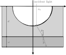
The HP arrays can make the light scatter and diffract in the glass, and increase the incident angle of light and the optical path length in the absorbing layer. Figure 9 shows the schematic diagram of light in a cell, where x0 is the incident position of light, lopt is the path length of light, θ 1 and θ 2 are the incident angle of light in glass and the refracted angle of light in the cell, ω and d are the thickness values of silicon and glass, respectively. So the path length of light is related to the incident position of light by

where sin θ 1 = n1x0/n2.
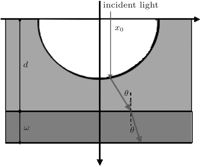 | Fig. 9. Schematic diagram of light path in the HP glass and silicon. |
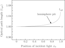
Figure 10 shows the relationship among the incident position of light x0, the thickness of cell ω , and the path length of light lopt. We can see that lopt increases definitely through the refraction of glass with an HP structure. The increment of path length, which refers to the position of incident light, is very limited, only close to the edge of the pit, the increment becomes obvious. Based on statistical theory, the average optical path length 〈 lopt〉 can be expressed as

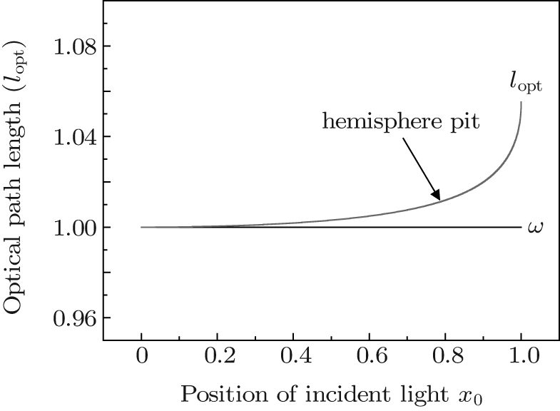 | Fig. 10. Relationships among the incident position of light x0, the thickness of cell ω , and the path length of light lopt. |
According to Eq. (12), we can also obtain the values of average incident angle and refracted angle as

Thus it can be seen that the average refracted angle is typically very small because the refractive index of silicon is considerably larger than the refractive index of glass.
According to the above discussion of the average optical path length, the percentages of transmitted light and reflected light, we can estimate the total optical path length of light in solar cells by using the calculation method of the Lambert surface as follows:[27, 28]

For ptra = 68.7%, pref = 31.3%, and lopt = 〈 lopt〉 = 1.006908ω , the above equation is convergent and obtained as

This result shows that the total optical path length in thin film Si solar cell increases to 4ω from the original 2ω by the HP glass. It means that, using this HP glass, the total path length of light is increased twice. This is very important to reduce the thickness of the absorbing layer of the cell and the manufacture cost of thin film solar cells, although the doubled optical path cannot obviously enhance the conversion efficiency of cells.
In this article, a numerical approach is taken to study the light trapping characteristics of the HP glass substrate. The research results show that the HP glass has good antireflection properties. By using this HP glass, the surface reflectivity can be reduced by about a half, and the unabsorbed light can return to the absorbing layer of the cell and produce the second absorption. The percentages of the second absorption light and the transmission light are 31.3% and 68.7%, so the HP glass can effectively reduce the total reflectivity of light from 20% to 13% in cells. The relative reduction of total reflectivity in the HP glass goes up to 35% as compared with the reflectivity of the planar glass. The HP glass can also prolong the optical path length in the thin film Si solar cell from original 2ω to 4ω . These results are in basic agreement with our experiment results.
Through the research in this paper, we can see that the HP glass has good characteristics of light trapping. For thin film silicon solar cells, not only can the HP glass substrate provide excellent antireflection properties, but also greatly prolong the optical path length. Moreover, the HP glass offers a way to improve the efficiency not by changing the microelectronic fabrication methods nor altering the device chemistry, but only by simply adding an HP glass onto the front glass of solar cells. Another major advantage is that it avoids forming the cracks during the growth of the layers, therefore the open-circuit voltage and the fill factor are not affected by the backside structure. The results of this paper provide a good idea to investigate the light trapping characteristics in the large-scale optical structure.
| 1 |
|
| 2 |
|
| 3 |
|
| 4 |
|
| 5 |
|
| 6 |
|
| 7 |
|
| 8 |
|
| 9 |
|
| 10 |
|
| 11 |
|
| 12 |
|
| 13 |
|
| 14 |
|
| 15 |
|
| 16 |
|
| 17 |
|
| 18 |
|
| 19 |
|
| 20 |
|
| 21 |
|
| 22 |
|
| 23 |
|
| 24 |
|
| 25 |
|
| 26 |
|
| 27 |
|
| 28 |
|