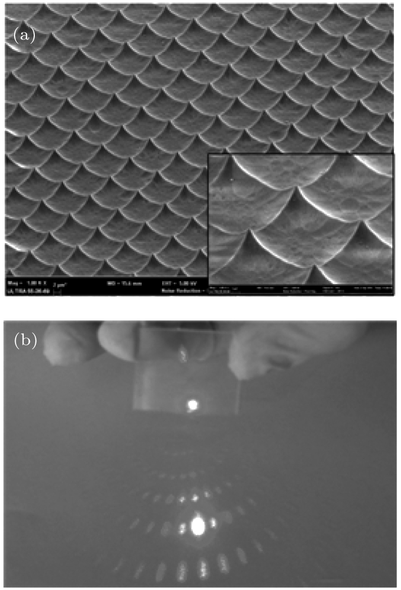
Light trapping characteristics of glass substrate with hemisphere pit arrays in thin film Si solar cells
Chen Lea), b) , Wang Qing-Kanga)†  , Wangyang Pei-Hua
a) , Huang Kuna) , Shen Xiang-Qiana)
, Wangyang Pei-Hua