Dynamic resistive switching in a three-terminal device based on phase separated manganites*
[Wang Zhi-Qiangb), a) , Yan Zhi-Boa)†  , Qin Ming-Hui
b) , Gao Xing-Senb) , Liu Jun-Minga)‡ ]
, Qin Ming-Hui]
|
|


†Corresponding author. E-mail: zbyan@nju.edu.cn
‡Corresponding author. E-mail: liujm@nju.edu.cn
*Project supported by the National Basic Research Program of China (Grant No. 2011CB922101), the National Natural Science Foundation of China (Grant Nos. 51301084 and 11234005), the Natural Science Foundation of Jiangsu Province, China (Grant No. BK20130576), and Program for Changjiang Scholars and Innovative Research Team in University, China (Grant No. IRT1243).
A three-terminal device based on electronic phase separated manganites is suggested to produce high performance resistive switching. Our Monte Carlo simulations reveal that the conductive filaments can be formed/annihilated by reshaping the ferromagnetic metal phase domains with two cross-oriented switching voltages. Besides, by controlling the high resistance state (HRS) to a stable state that just after the filament is ruptured, the resistive switching remains stable and reversible, while the switching voltage and the switching time can be greatly reduced.
Recently, reversible resistive switching (RS) in metal/oxide/metal sandwiched structures has attracted great attention due to its potential for making high performance resistance random access memories (RRAM).[1– 5] By applying voltage pulses, the resistances of the devices can be reversibly switched between nonvolatile high resistance state (HRS) and low resistance state (LRS).[1, 2] The formation/rupture of the conductive filaments in the oxide matrix is one of the usual ways to realize this RS behavior.[1] For many freshly fabricated RRAM cells, a forming process, in which a forming voltage (Vform) develops initially conductive filaments inside the insulator layer, is usually needed to active the memory cell before the memory cell can work. Then, a reset process, in which a reset voltage (Vreset) ruptures the filaments, switches the cell from LRS to HRS. Next, another set voltage (Vset) re-captures the filaments and switches the cell from HRS to LRS again, which is denoted as the set process. During the forming and the set processes, a compliance current is used to limit the possible big avalanche current to avoid damaging the memory cell.
Many experimental and theoretical investigations have reported that conductive filaments can be formed/ruptured by the redox of metal ions and/or the migration of oxygen vacancies in the oxide matrix.[1– 3] This ion-migration-related filament-type switching mechanism usually has good retention, high off/on ratio, and nanosecond-scale switching speed. However, the random formation/rupture of filaments at non-controllable local regions usually leads to large fluctuations on both the endurances and the critical switching voltages, which greatly hinders the actual memory applications.[1– 3]
Alternatively, the voltage can form/rupture filaments by changing and/or reshaping the metallic electronic phases in strongly correlated electron systems without long-range migration of the ions/vacancies.[4– 6] This mechanism, if applicable, would offer a highly favored advantage in terms of switching speed because electron hopping is much faster than ionic migration. As one of the most investigated electron phase separated manganites, (La1− yPry)1− xCaxMnO3 displays a first-order electronic phase transition between ferromagnetic metallic (FMM) and charge-ordered insulating (COI) phases, and exhibits wide liquid-like and frozen phase separation (PS) temperature regions, in which the external stimuli can easily tune the transport behavior of the system.[7– 11] A small voltage or current reshapes the FMM phase domains, and finally leads to the formation of conductive filaments along the electric field direction by the intrinsic electronic effect.[6, 12– 16] However, with a large electric field applied, the remarkably parasitic Joule heating in the filament regions can dramatically increase the temperature in the local regions.[4, 6] Due to the first-order electronic phase transition nature, the Joule heating induced local annealing of the system would result in different frozen PS structures and lead to different nonvolatile resistance states at low temperature.
Since the first-order electronic phase transition can be well controlled by both the electric field and the annealing processes, the resistive switching based on such a mechanism in electronically PS manganites should be more stable than that based on the non-controllable ion-migration mechanism. The stable RS behavior based on the electronic phase transitions in La0.225Pr0.4Ca0.375MnO3 has been experimentally presented in earlier investigations.[4, 12] However, in such an electronic phase transition switching mechanism, the Joule heat annealing usually needs a large current and has a long relaxation time (in tens of seconds time scale), which means large energy consumption and long operation time, respectively. Since the parasitic Joule heating effect is ignored in the Monte Carlo simulations, the electric field with a fixed direction can form the FMM filaments but cannot rupture them.[13] To solve this problem, we suggest a three-terminal memory device based on La0.225Pr0.4Ca0.375MnO3 and study the reversible RS using Monte Carlo (MC) simulations based on the dielectrophoresis model. Our result indicates that by reshaping the FMM domains, the conductive filaments can be formed and annihilated by two cross-oriented switching voltages, respectively. With this controlling protocol, large Joule heating can be avoided, and the switching voltage and the switching time can be effectively reduced.
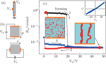
Figure 1(a) shows a schematic drawing of the 3-terminal device. The device is set (from HRS to LRS) by a vertical voltage Vy and reset (from LRS to HRS) by a horizontal voltage Vx. The resistances of the device are read via the Vy terminal, i.e., the HRS or LRS states are determined by the y-direction resistance Ry. To model the electronically PS structure, we start from a two-dimensional square lattice (L × L, L = 50), where each bond represents an electronic phase (FMM or COI). Therefore, this lattice is more or less a coarse-grained model of the realistic PS structure in (La1− yPry)1− xCaxMnO3. As shown in Fig. 1(b), the voltage Vy is applied in the y direction to form conductive paths, while the voltage Vx is applied along the x direction to annihilate the filaments, which is equivalent to the 3-terminal configuration in Fig. 1(a).
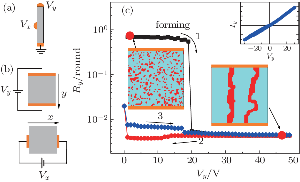 | Fig. 1. (a) Schematic drawing of the 3-terminal memory device. (b) Illustration of the device configurations during the simulation processes. (c) The Vy dependent y-directional resistance Ry. The top-right inset shows the Iy– Vy behavior after the forming process. Left and bottom insets are the snapshots of PS at the initial and the final states, respectively. Red and cyan sites represent the metallic and the insulating phases, respectively. |
In our MC simulation, a standard Metropolis algorithm is used with a dielectrophoresis mechanism. Considering the fact that the conversion between FMM and COI phases can be ignored after the application of a low electric field (< 106 V/m), the fixed fraction (pM) of “ flowable” FMM phase sites in the insulating matrix can describe the PS structure in manganites.[12, 13, 17] The exchange between the nearest neighboring (NN) lattice sites is proportional to the probability determined by the free energy change. The total free energy can be written as[13]

where FE denotes the electric energy; the dielectric constant ε (r) equals ε M(r) or ε I(r) when r locates in the metallic phase or the insulating phase, respectively; and, FS represents the interface energy between metallic and insulating phases, and is proportional to the interfacial area S with a coefficient A. The local field E(r) and the resistance Ry along the y direction can be calculated using the resistor-network (RN) model, [18– 20] in which three types of resistors are distributed according to the bonds (links) between the NN sites: RM between metallic sites, RI between insulating sites, and RMI between a metallic site and an insulating site. For simplification, we have RMI = (RM+ RI)/2 here.[20] The voltage at each site V(r) is obtained by solving the Kirchhoff equations and E(r) is the negative gradient of V(r). To accelerate the calculation the RI/RM ratio and the ε M/ε I ratio are assumed to take the same value f (≫ 1). The simulation is performed at a fixed temperature. The parameters used in our simulation are listed in Table 1. The system evolves as time passes, e.g., Monte Carlo steps (MCS).
| Table 1. The parameters used in the model. Here, the selection of pM, which is within the reasonable range (Ref. [11]), mostly benefits the RS and can lead to the smallest switching times during the filament forming/rupture processes. The value of f is within the experimental range for manganites (Refs. [4] and [8]). The other parameters are relative values. |
In the vertical direction, the Vy-dependent resistance Ry is shown in Fig. 1(c). The left inset in Fig. 1(c) shows the initial HRS state, in which the metallic sites (red regions) are distributed randomly in the insulating matrix (cyan regions). With the increase of Vy from zero, Ry first remains at the HRS, then dramatically drops to an LRS at Vy ∼ 20, and finally keeps at the LRS even when Vy ∼ 50, being qualitatively consistent with the previously experimental results.[6, 12] The lower right inset in Fig. 1(c) shows that the metal phase domains have been reshaped by Vy and aligned into the conductive filaments along the y direction as Vy ∼ 50. Hence, the forming of the filaments explains the dramatic drop of Ry at Vy ∼ 20. Next, as Vy is retracted from 50 to 0, and then re-increased to 50, Ry always remains at the LRS, indicating that the Vy-induced resistance switching is nonvolatile. In addition, the Ohmic Iy– Vy behavior in the upright inset of Fig. 1(c) shows that the resistance of the LRS is almost Vy-independent, even with reversing the polarity of Vy.
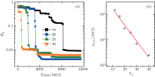
Due to the existence of a remarkable aging effect in PS manganites, the resistance of the system also strongly depends on the dynamic evolution history.[9] Here, we simulate the time dependent Ry under the stressing of different Vy. For the different Vy situations, the simulations all start from the same initial HRS state. Figure 2(a) shows the time dependent Ry behaviors with Vy = 30, 25, 20, and 16 respectively. With initial Vy = 30, Vy suddenly drops to the LRS in a forming time tform = 680 MCS. With the decrease of Vy, the suddenly drop of resistance still appears but tform increases exponentially, as shown in Fig. 2(b), which is consistent with a dynamic percolation scenario.[6, 12, 14] Hence, the time needed for forming the conductive filament is determined by the amplitude of Vy.
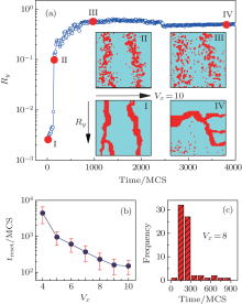
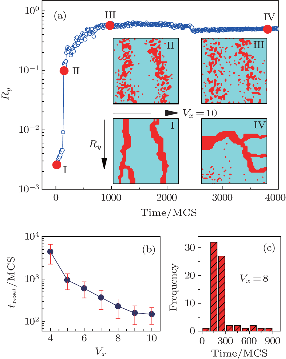
On the other hand, to annihilate the y-direction filament and switch the system back to the HRS, we apply a constant voltage Vx = 10 along the x direction and then calculate Ry. The time dependent Ry and the snapshots of PS at t = 0, 140, 1000, and 3800 (MCS) are shown in Fig. 3(a) and the insets, respectively. At the beginning of applying Vx, the filaments along the y direction remain and Ry stays at the LRS. With the lapse of time, the filaments start to be dissolved and Ry displays a dramatic jump to a high value at a critical time, i.e., the reset time treset = 140, and then continues with a small increase until t = 1000, obtaining the stable HRS. With further increase in the evolution time to above 3800 MCS, the y-direction filaments are completely dissolved while the filaments along the x direction come into being on the contrary. Therefore, the LRS can be reset to the HRS by applying a voltage along the x direction with enough time.
 | Fig. 2. The forming process. (a) Time dependent Ry under the stressing of different Vy. (b) The Vy dependent forming time tform. Here tform is defined as the time when a dramatic resistance drop occurs. |
Besides, in the reset process from LRS to HRS, treset strongly depends on the value of Vx. To reveal this relationship, we simulate and calculate the time dependent Ry under the stressing of different Vx. The simulation and calculation are repeated 69 times for data reliability. Figure 3(b) indicates that treset quickly decreases with increasing Vx. This is a reasonable result since the larger Vx can provide a larger dielectrophoresis force to disrupt the y-directional filaments. Figure 3(c) shows the count distribution of treset at Vx = 8. The distribution indicates that treset is usually between 150 and 250 (MCS) in the 1000 MCS simulations, which evidences the reliability of the data in Fig. 3(b).
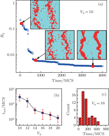
For actual applications, it is beneficial to reset the device from LRS to HRS within a short time and by a small voltage. For the reset process in Fig. 3(a), treset ∼ 150 MCS and hence the usage of t = 1000 MCS is long enough to obtain a stable HRS. At this HRS, the y-directional filaments are ruptured but the metallic domains still mainly distribute in the regions nearby the previous filaments. To study how such HRS affects the next following switching from HRS to LRS, we again apply Vy = 16 in the vertical direction and calculate the time-dependent Ry.
The simulation results, shown in Fig. 4(a) and its insets indicate that the disrupted filaments are re-captured and the system is set to the LRS again after a proper time, which is similar to the forming process shown in Fig. 2(a). However, one can easily find that the tset needed for re-capturing the filaments is only ∼ 620 MCS, which is much shorter than tform (tform ∼ 8200 MCS) in Fig. 2(a). This suggests that, by controlling the HRS to a stable state just after the filaments are ruptured, the re-capture of the filaments becomes much easier and tset is remarkably reduced.
 | Fig. 3. The reset process. (a) The calculated Ry as a function of time, with the stressing of Vx = 10. The insets are four snapshots of the PS states at different times. (b) The Vx dependent reset time treset. (c) The count distribution of treset at Vx = 8, with 69 repeated simulations. |
We have also studied the Vy-dependent tset. The simulation starts from an HRS state with the PS structure shown in the left inset of Fig. 4(a), and is carried out by monitoring the evolution of the PS structure under the stressing of different Vy. Figure 4(a) indicates that tset also decreases with increasing Vy, which is similar to the dependency of treset with Vx. By comparing the forming processes under different situations shown in Fig. 2(b), one can easily find that tset is always smaller than tform whatever Vy is. Figure 4(c) shows the count distribution of tset in the 51 repeated simulations within 1000 MCS at Vy= 16, in which tset < 700 MCS and is mainly distributed between 150 MCS and 250 MCS.
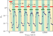
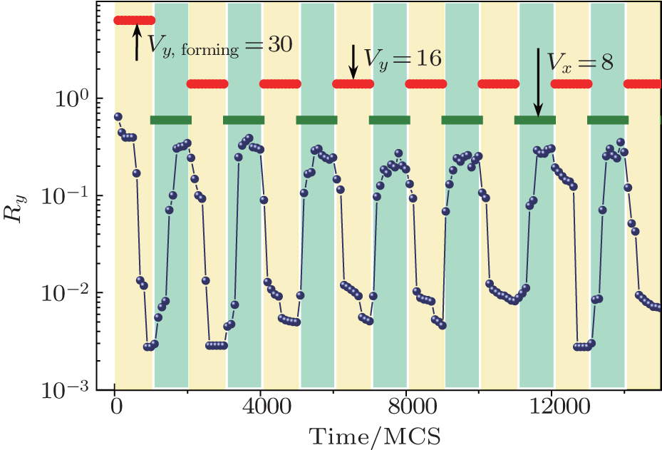
Therefore, the switching time can be reduced by increasing the switching voltage and can be further reduced by choosing a proper HRS. According to this result, one can select suitable forming, set, and reset voltages to produce the reversible RS between stable HRS and LRS within 1000 MCS. To verify this conclusion, we simulate the continuously reversible RS that starts from the initial HRS state shown in the left inset of Fig. 1(c). To obtain the conductive filaments from the initial HRS state within 1000 MCS, Vy = 30 is used as the forming voltage. In the simulation, Vy = 16 and Vx = 8 are used as the set and the reset voltages, respectively, and they are alternatively applied to the device with a fixed duration of 1000 MCS.
 | Fig. 4. The set process. (a) The calculated Ry as a function of time, with the stressing of Vy = 16. The insets are three snapshots of the phase separation states at different times. (b) The Vy dependent set time tset. (c) The count distribution of tset at Vy = 16, with 51 repeated simulations. |
 | Fig. 5. Time dependent reversible resistive switching with alternative applying Vx and Vy pulses respectively. The pulse durations are fixed to 1000 MCS. |
Figure 5 shows the simulation result, in which the continuously reversible and stable RS is clearly displayed. It needs to be addressed that both the HRS and the LRS are stable and have good retentions after the turn-off of the set and the reset voltages since the PS state in manganites below ∼ 30 K is frozen.[6]
Our simulation results indicate that applying larger operation voltages Vx and Vy can effectively reduce the switching times, including tset and treset. In the actual memory application, however, a large operation voltage not only leads to a large energy consumption but also produces remarkable Joule heating that would extend the switching time and weaken the RS stability on the contrary. This happens because the Joule heating induced increase of temperature would lead the system into a liquid-like PS state with a much more remarkable aging behavior, even though no external voltage is applied.[9] Therefore, the Joule heating limits the maximum applicable operation voltages.
It can be imaged that the operation voltage and the switching time are also dependent on the sizes of the system. The previous investigation has revealed that the FMM filaments in (La1− yPry)1− xCaxMnO3 can be formed in the nanometer scale.[21] A sample device with a size of a hundred-nanometers can be designed to effectively reduce the number of filaments inside the device. In such a small device, by assuming that the electric field intensity for resistive switching is fixed, the few filaments with nanometer scale size greatly reduce the switching voltages. By using the parameters taken from the experiments, [4, 5, 11, 12] the resistivity of the filament is calculated to be ρ ∼ 104 Ω · m, and the critical electric field that forms the filament in Fig. 1(c) is estimated to be Ec ∼ 103 V/m. By assuming that the device size is l = 100 nm and the filament formed inside it has a diameter of d = 20 nm, it can estimated that the switching voltage Vc = lEc ∼ 10− 4 V and the heating power 
We have studied the resistive switching of a 3-terminal device based on the electric phase separation manganites by using Monte Carlo simulations with the dielectrophoresis model. Our result indicates that the conductive filaments can be formed and annihilated by two cross-oriented switching voltages Vy and Vx, respectively. By using this control, the reversible and stable resistive switching between HRS and LRS is demonstrated. Our simulation also indicates that both the set and the reset times decrease with increasing switching voltages. Besides, by controlling the HRS to a stable state just after the rupture of the conductive film, both the switching voltages and the switching times can be further reduced. Based on the PS manganites, a nanometer-scale 3-terminal device is suggested to produce a high performance resistive switching behavior.
The electrical modulation of the electronic metal phase is an important mechanism for reliable resistance switching because the electronic migration is much faster than the ionic migration. We believe that the electrical modulation of the electronic metal phase is a general mechanism and should be observed in many electronic phase-separated oxides. With this electronic switching mechanism, we believe that the method with two cross-oriented switching voltages can be applied to realize reversible resistance switching between HRS and LRS in many oxides.
| 1 |
|
| 2 |
|
| 3 |
|
| 4 |
|
| 5 |
|
| 6 |
|
| 7 |
|
| 8 |
|
| 9 |
|
| 10 |
|
| 11 |
|
| 12 |
|
| 13 |
|
| 14 |
|
| 15 |
|
| 16 |
|
| 17 |
|
| 18 |
|
| 19 |
|
| 20 |
|
| 21 |
|