|
|
Dynamic resistive switching in a three-terminal device based on phase separated manganites*
|
Wang Zhi-Qiang b),a), Yan Zhi-Bo a)† , Qin Ming-Hui b), Gao Xing-Sen b), Liu Jun-Ming a)‡ |
|
| |
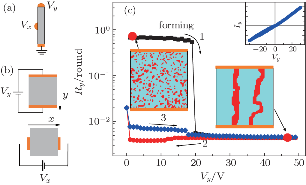
| (a) Schematic drawing of the 3-terminal memory device. (b) Illustration of the device configurations during the simulation processes. (c) The V y dependent y -directional resistance R y . The top-right inset shows the I y – V y behavior after the forming process. Left and bottom insets are the snapshots of PS at the initial and the final states, respectively. Red and cyan sites represent the metallic and the insulating phases, respectively. |
|
|
 |
|
|