
Improved performance of AlGaN/GaN HEMT by N2O plasma pre-treatment*
[Mi Min-Han, Zhang Kai, Zhao Sheng-Lei, Wang Chong, Zhang Jin-Cheng, Ma Xiao-Hua, Hao Yue† ]
]
]
|
|


Corresponding author. E-mail: yhao@xidian.edu.cn
Project supported by the National Natural Science Foundation of China (Grant No. 61334002) and the Opening Project of Science and Technology on Reliability Physics and Application Technology of Electronic Component Laboratory, China (Grant No. ZHD201206).
The influence of an N2O plasma pre-treatment technique on characteristics of AlGaN/GaN high electron mobility transistor (HEMT) prepared by using a plasma-enhanced chemical vapor deposition (PECVD) system is presented. After the plasma treatment, the peak transconductance ( gm) increases from 209 mS/mm to 293 mS/mm. Moreover, it is observed that the reverse gate leakage current is lowered by one order of magnitude and the drain current dispersion is improved in the plasma-treated device. From the analysis of frequency-dependent conductance, it can be seen that the trap state density ( DT) and time constant ( τT) of the N2O-treated device are smaller than those of a non-treated device. The results indicate that the N2O plasma pre-pretreatment before the gate metal deposition could be a promising approach to enhancing the performance of the device.
The development of AlGaN/GaN high electron mobility transistors (HEMTs) has been largely advanced in recent years, leading to the improvement of microwave power performance.[1, 2] Even with the AlGaN/GaN HEMTs emerging as a feasible technology for high frequency and high power amplifiers, there are still several problems to be solved. One of the key problems is the Schottky gate HEMT suffers serious gate leakage current, which may not only impede device reliability but also degrade power efficiency.[3] One approach to suppressing the gate leakage current is to add an insulator dielectric layer between the gate metal and the AlGaN layer. However, with the additional insulating gate dielectric, the additional process steps of dielectric deposition and patterning are needed to form the structure. In addition, the threshold voltage is shifted more negatively, [4] and the maximum transconductance is reduced, owing to the increased distance from the gate to the channel.[5– 7] Another problem is the drain current dispersion, which degrades the output power performance and small-signal characteristics.[8] It has been found that the plasma pre-treatment of the AlGaN surface before the gate metal deposition can reduce the leakage current level.[9] Plasma treatment such as C2F6 or CF4 can effectively reduce the leakage current, but an undesirable side effect of this process reduces the channel conductivity.[10]
In this paper, we investigate the influence of N2O plasma pre-treatment of the AlGaN surface before the gate metal deposition on the electrical performance in AlGaN/GaN HEMT. The focus is placed on the electrical performance associated with a Schottky gate with using the N2O plasma pre-treatment for non-plasma pre-treatment as a reference. Particular interest for the discussion is how the plasma pre-treatment affects the performance of the device. Finally we adopt the frequency-dependent conductance analysis to investigate the trap states before and after the treatment of AlGaN/GaN HEMTs.
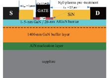
The AlGaN/GaN HEMTs used in this paper were grown on sapphire substrates by metal– organic chemical vapor deposition (MOCVD). The schematic cross section of the plasma pre-treated AlGaN/GaN HEMT is shown in Fig. 1. The HEMT consisted of a low-temperature AlN nucleation layer and a 1.4-μ m unintentionally doped GaN buffer layer. Finally a 20-nm AlGaN barrier layer with an Al mole fraction of 30% and 1.5-nm GaN cap layer were deposited. Adding a GaN cap layer to the AlGaN/GaN structure can reduce the Ohmic contact resistance. Room-temperature Hall measurements showed an electron sheet concentration of 9.8 × 1012 cm− 2 and a mobility of 1983 cm2/V· s, resulting in a sheet resistance of 318 Ω /◽ .
 | Fig. 1. Schematic cross section of N2O plasma pre-pretreated AlGaN/GaN HEMT. |
In our studies, the device fabrication started with the formation of a source/drain contact with Ti/Al/Ni/Au (22 nm/140 nm/55 nm/45 nm) by electron beam evaporation and annealed in N2 ambient at 830 ° C for 30 s. Using the on-wafer transfer length method (TLM), the Ohmic contact resistance was measured to be 0.3 Ω · mm. Then, a 120-nm mesa etched by Cl2-based reactive ion etching (RIE) was used as a device region. The buffer leakage current was as low as 1.8 × 10− 4 mA/mm between two isolated mesas at a distance of 5 μ m and the voltage across the two isolated mesas was 100 V. After 60-nm SiN deposition on the surface of the device by plasma-enhanced chemical vapor deposition (PECVD) to reduce frequency dispersion, the plasma pre-treatment window with 1.7-μ m length was opened by contacting the photolithograph, and then etched by CF4 plasma in an RIE system at a radio frequency (RF) power of 50 W to remove the SiN out of the plasma pre-treatment region. A PECVD system was used for N2O plasma pre-treatment before the gate metal deposition. For the N2O treatment, the flow rates of N2O and N2 were 50 sccm and 100 sccm respectively, the chamber pressure was 600 mTorr (1 Torr = 1.33322 × 10² Pa), the RF power was 18 W, and the chamber temperature was 250 ° C. Finally the gate window with a 0.5-μ m footprint length was opened by contacting the photolithograph, and then an Ni/Au/Ni (45 nm/200 nm/20 nm) gate electrode was deposited by electron beam evaporation. Two types of devices are investigated in this paper. Both are fabricated in the same process except that the barrier layer under the gate is plasma-treated. Each of the devices in this paper has a gate width of 50 μ m, a gate– source spacing of 1 μ m, and a gate– drain spacing of 2.5 μ m. In addition, circular shape Schottky barrier diodes (SBDs), each with a circular gate contact having a diameter of 130 μ m and surrounding Ohmic contact with an Ohmic-Schottky separation of 30 μ m, are used for measuring the frequency-dependent capacitance and conductance.
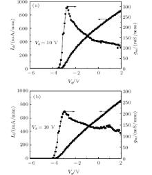
The transfer characteristics of the plasma-treated and non-treated HEMTs are shown in Fig. 2. We define Vth as the gate bias intercept of the linear extrapolation of drain current at the point of peak transconductance (gm). The values of Vth are, respectively, − 3.2 V for the plasma-treated HEMT and − 3.5 V for the non-treated HEMT, which can be neglected between the two kinds of HEMTs. The peak transconductance (gm) of the non-treated HEMT is 209 mS/mm. In contrast, the peak gm of the plasma-treated HEMT is 293 mS/mm. The values of maximum drain current (Id) are 865 mA/mm and 860 mA/mm for plasma-treated and non-treated HEMTs, respectively. Schottky diode characteristics are shown in Fig. 3(a). Under a negative gate bias Vg = − 20 V, the gate leakage current (Ig) of plasma-treated HEMT is as low as 3.67 × 10− 2 A/cm2, which is approximately one order of magnitude smaller than that of the non-treated HEMT. The breakdown voltage Vbr is measured under a deep closed-gate condition when the Vg = − 8 V is less than Vth. The Vbr is defined as the voltage at which the drain leakage current Id reaches 1 mA/mm. Figure 3(b) shows the DC breakdown characteristics. The off-state breakdown voltages are 105 V and 83 V for plasma-treated and non-treated HEMTs, respectively. It can be obviously seen that gate leakage current Ig and drain leakage current Id dramatically increase at the same time when the drain voltage Vd exceeds 80 V for the non-treated HEMT. For the non-treated HEMT, in the vicinity of the breakdown voltage, the Ig is about 0.6 mA/mm, which is larger than the buffer leakage current. This means that the breakdown of the HEMT is induced by the gate leakage current. In contrast, the gate leakage current Ig of the plasma-treated HEMT remains low when the Vd exceeds 100 V. This suggests that the suppression of the gate leakage current is responsible for the enhanced breakdown voltage of the plasma-treated HEMT.
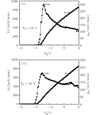 | Fig. 2. Transfer characteristics of (a) N2O plasma-pre-treated and (b) non-treated HEMTs at Vd − 10 V. |
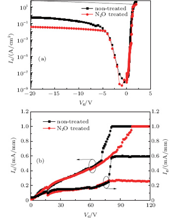 | Fig. 3. (a) Schottky diode characteristics and (b) DC breakdown characteristics. |
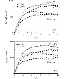
Pulsed measurements are performed by using the pulse of 0.5 μ s in width and 100 μ s in period (Fig. 4) applied to the gate electrode to investigate the current dispersion of the device. At the bias point (VGSQ, VDSQ) = (− 8 V, 0 V), there is a potential difference between gate and drain, so the electrons in the gate electrode could be captured by the trap state. Therefore, the bias point (VGSQ, VDSQ) = (− 8 V, 0 V) is selected to evaluate the trap state and avoid the self-heating effect. Figure 4 shows that a 10.8% drain current (Id) reduction of the non-treated device happens at VGS = 2 V and VDS = 10 V while the device treated by N2O plasma shows a 3.3% increase of drain current due to the reduced self-heating effect. The results indicate that the N2O plasma pre-treatment can essentially suppress the trap state-related carrier trapping and could help improve the high frequency characteristics of the devices.
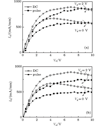 | Fig. 4. Comparison of pulsed I– V characteristics between (a) with and (b) without N2O plasma pre-treatment at point of (VGSQ, VDSQ) = (− 8 V, 0 V). |
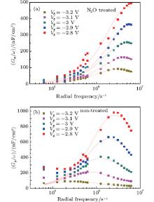
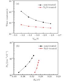
In order to further investigate how the N2O plasma pre-treatment improves the performance of the device, we conduct frequency-dependent conductance measurements to study the variations of trap states in the devices with and without N2O plasma treatment.[11] Plots of Gp/ω versus ω for the two devices at selected gate bias are shown in Fig. 5. The trap state density DT and the time constant τ T could be extracted by fitting the measured parallel conductance Gp as a function of ω according to equation

where ω = 2π f is the radial frequency, Gp/ω has a maximum at ω = 2/τ T and at that maximum DT = 2.5Gp/qω . The variations of the time constant of the trap state with the gate voltage evaluated for the two devices are shown in Fig. 6(a). With the gate voltage increasing from − 3.2 V to − 2.8 V, trap time constants decrease from 0.636 μ s to 0.318 μ s for plasma-treated and from 10.6 μ s to 0.796 μ s for non-treated devices, respectively. The variations of trap state density with the energy level are plotted in Fig. 6(b). The trap state energy ET could be found using the time constant resulting from the fitting procedure and considering that τ T = (σ TNcυ T)− 1exp(ET/kT), where the capture cross section of the trap state σ T = 3.4 × 10− 15 cm− 2, the density of states in the conduction band Nc = 2.2 × 1018 cm− 3, and the average thermal velocity of the carriers υ T = 2.6 × 1017 cm/s are used. For N2O plasma-treated devices, trap state densities of 1.41 × 1012 cm− 2· eV− 1– 7.7 × 1012 cm− 2· eV− 1 are located at ET in a range of 0.305 eV– 0.286 eV. In contrast, a trap state density of 1.4 × 1012 cm− 2· eV− 1– 1.53 × 1013 cm2· eV− 1 is located at ET in a range of 0.378 eV– 0.31 eV in the non-treated devices.
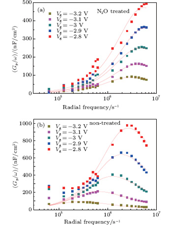 | Fig. 5. Variations of conductance with radial frequency for (a) N2O and (b) non-N2O treated HEMTs at selected gate voltages. |
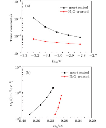 | Fig. 6. (a) Plots of trap state time constant versus gate voltage, and (b) plots of trap state density versus energy for N2O-treated and non-N2O-treated devices. |
It is noted that in the N2O plasma-pre-treated devices, the densities of the trap states are reduced, and simultaneously the time constants of the trap states are also reduced. The reduced trap state time constant could explain the suppression of drain current dispersion after the N2O plasma pre-treatment. In the pulsed measurements, the traps could capture electrons near the gate. The trapped electrons could deplete the channel near the drain side of the gate edge, thus resulting in the drain current dispersion. At the bias point (VGSQ, VDSQ) = (− 8 V, 0 V), the gate electrons are excluded to fill the trap states near the drain side of the gate edge. Because the time constants of trap states in N2O-treated devices are less than those of non-treated devices, the trapped electrons in N2O-treated devices could be kept there until the gate voltage changes to a value at which electrons are de-trapped. Therefore, the drain current (Id) dispersion in an N2O-treated device could be suppressed. The trap assistant tunneling is the dominant source of reverse gate leakage current (Ig), so the decrease of trap density by N2O plasma treatment is the reason for suppressing the reverse gate leakage current. The increase of peak transconductance (gm) could also be attributed to the decreasing of trap density and time constant, thus enhancing the ability to control the gate of the channel. In Ref. [12], a 0.37-eV deep level trap state seems to be an N vacancy or a complex related to the N vacancy. After the N2O plasma pre-treatment, the trap state energy around 0.37 eV is removed. Although the trap states still exist, the energy levels of the remaining trap states are shallow, so they cannot suppress the performance of the device. This means that N2O plasma pre-treatment partially recovers the N-vacancy-related surface defects, thereby leading to the reduction of trap states.[13] We assume that the improvement in performance of the N2O-treated device is attributed to this reason.
In this paper, we report on the N2O-treated and non-treated devices fabricated on one wafer. It is found that N2O plasma treatment could improve the peak transconductance and off-state breakdown voltage, suppress the reverse gate leakage current and drain current dispersion. Frequency-dependent conductance analyses of these devices are conducted to investigate the reason for N2O plasma pre-treatment improving the performance of the devices. These analyses show that the trap state density (DT) and time constant (τ T) of the N2O-treated device are smaller than those of the non-treated device. These results demonstrate the great potential of using N2O plasma pre-pretreatment to improve the performance of devices.
| 1 |
|
| 2 |
|
| 3 |
|
| 4 |
|
| 5 |
|
| 6 |
|
| 7 |
|
| 8 |
|
| 9 |
|
| 10 |
|
| 11 |
|
| 12 |
|
| 13 |
|