Observation of magnetoresistance in CrI3/graphene van derWaals heterostructures*
Project supported by the National Natural Science Foundation of China (Grant No. 51872039) and Science and Technology Program of Sichuan, China (Grant No. M112018JY0025).
Niu Yu-Ting1, 2, Lu Xiao1, 2, Shi Zhong-Tai1, 2, Peng Bo1, 2, †
ManuID:
ac1e1d
Received:2021-06-01
Copyright:
2021
More
Abstract
Two-dimensional ferromagnetic van der Waals (2D vdW) heterostructures have opened new avenues for creating artificial materials with unprecedented electrical and optical functions beyond the reach of isolated 2D atomic layered materials, and for manipulating spin degree of freedom at the limit of few atomic layers, which empower next-generation spintronic and memory devices. However, to date, the electronic properties of 2D ferromagnetic heterostructures still remain elusive. Here, we report an unambiguous magnetoresistance behavior in CrI3/graphene heterostructures, with a maximum magnetoresistance ratio of 2.8%. The magnetoresistance increases with increasing magnetic field, which leads to decreasing carrier densities through Lorentz force, and decreases with the increase of the bias voltage. This work highlights the feasibilities of applying two-dimensional ferromagnetic vdW heterostructures in spintronic and memory devices.
Keywords:two-dimensional ferromagnetic
;
van der Waals heterostructure
;
magnetoresistance
;
NiuYu-Ting, LuXiao, ShiZhong-Tai, PengBo. Observation of magnetoresistance in CrI3/graphene van derWaals heterostructures*
Project supported by the National Natural Science Foundation of China (Grant No. 51872039) and Science and Technology Program of Sichuan, China (Grant No. M112018JY0025).
Controlling the spin degree of freedom is a vital foundation of spintronic devices and magnetic memory with ultralow energy consumption, ultrahigh speed and density in modern electronics. Graphene has provided a rich platform for exploiting spin controlling at the limit of single or few atomic layers,[1–4] which brokes the inherent cognition that two-dimensional monolayer could not stably exist at room temperature, which has exhibited plenty of unprecedented functions and unique properties, such as long spin lifetime, long spin transport distance and high carrier mobility,[5,6] allowing it to transmit and manipulate spin signals in complex multi-terminal device architectures.[7,8] This has enabled vast flexibility for creating graphene-based spintronic devices[9–12] and for cashing out values of graphene. Long-range ferromagnetic orders have recently been reported in diverse vdW ferromagnetic materials,[13–17] such as CrI3, Cr2Ge2Te6 and Fe3GeTe2.[18–22] This makes it possible to create a heterostructure comprising graphene and distinct two-dimensional (2D) vdW ferromagnetic materials to create spintronic devices with unique functions beyond the reach of isolated layered materials.[23–27] Magnetic proximity effect has been recently reported in CrBr3/graphene heterostructures, which show strong magnetic exchange leading to a significant Zeeman splitting field in graphene.
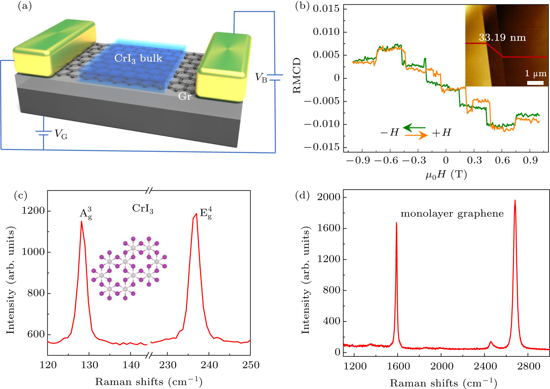
Here, we demonstrate a longitudinal magnetoresistance behavior with increasing external magnetic field in CrI3/graphene heterostructures. The magnetoresistance ratio is ∼ 2.8%. The magnetoresistance can be tuned by bias and gate voltage. With increasing bias voltage, the magnetoresistance decreases and the current increases; in contrast, a positive gate voltage decreases the magnetoresistance. A typical CrI3/graphene vdW heterostructure for electrical transport measurement is shown in Fig. 1(a). The CrI3 multilayers exfoliated from crystals by PDMS were transferred onto graphene. CrI3 is an Ising ferromagnet with out-of-plane spin orientation, showing strong out-of-plane magnetic anisotropy. The CrI3 monolayer exhibits ferromagnetism, and interlayer antiferromagnetic coupling leads to an antiferromagnetic arrangement in CrI3 bilayers.[28] The magnetism can be electrically controlled in CrI3 mono- and bi-layers through the magnetoelectric coupling effect.[29] The interfacial exchange coupling at the interface of CrI3 and graphene can significantly influence the electronic and optoelectronic properties of the layered crystals.[30–33] This study provides a platform for fundamental physics studies toward the next-generation 2D spin logic and memory devices.
Fig. 1. CrI3/graphene van der Waals heterostructures. (a) Schematic of CrI3/graphene heterostructures. (b) RMCD spectrum of CrI3 bulk. The inset is the AFM images. The scale bar is 1 μm. (c)–(d) Raman spectra of few-layer CrI3 and monolayer graphene. The inset in (c) is schematic atomic structure of CrI3 monolayer. Purple atoms: chromium; white atoms: iodide.
Methods
CVD-grown graphene was transferred onto the Au electrodes on SiO2/Si substrate through PMMA methods. The copper films for graphene growth were dissolved by FeCl3 solutions. Thick CrI3 bulk was exfoliated from crystal by PDMS films and further covered onto graphene in a glovebox. Agilent B1500 was used to record the magnetoresistance behaviors of the CrI3/graphene heterostructures. The Raman signals were recorded upon 514 nm light excitation by a Witec Alpha 300R Plus confocal Raman microscope. The power of the 514 nm excitation laser was ∼ 2 mW. The B1500 and Witec Raman system was coupled with closed cycle superconducting magnet and liquid helium cryostat for low-temperature optical and electrical measurements.
Results and discussion
CrI3 is a typical 2D ferromagnetic material. The plane of Cr atoms forms a honeycomb lattice and is sandwiched between two planes of I atoms. Each Cr atom is arranged at corner of the shared octahedron and is surrounded by 6 neighbor I atoms as shown in the insert of Fig. 1(c). Figure 1(b) shows a typical reflective magnetic circular dichroism (RMCD) spectrum of CrI3 bulk, indicating complex magnetic order properties of the CrI3 bulk. The AFM measurements show that the thickness of the CrI3 bulk is ∼ 33.2 nm. The Raman features of the CrI3 bulk and graphene were measured using our Raman confocal imaging system (Figs. 1(c) and 1(d)). Two vibration peaks at 127.8 cm−1 and 238.4 cm−1 are clearly observed in the CrI3 sample, which are assigned to and vibration modes, respectively. The mode represents the out-of-plane vibration of the I atom, and the mode represents the in-plane alternating displacement of the Cr atom. As shown in Fig. 1(d), the Raman spectrum of graphene displays typical G and 2D peaks. The G peak around 1580 cm−1 is the main characteristic peak of graphene, arising from in-plane vibrations of the sp2 bonded carbon atoms. The 2D peak appears at 2680 cm−1, which originates from the second-order zone-boundary phonons. The D peak which is generally considered to be the disordered vibration peak of graphene is negligibly observed. The full-width at half-maximum (FWHM) of the 2D Raman feature is ∼ 35 cm−1, which corresponds to monolayer graphene.
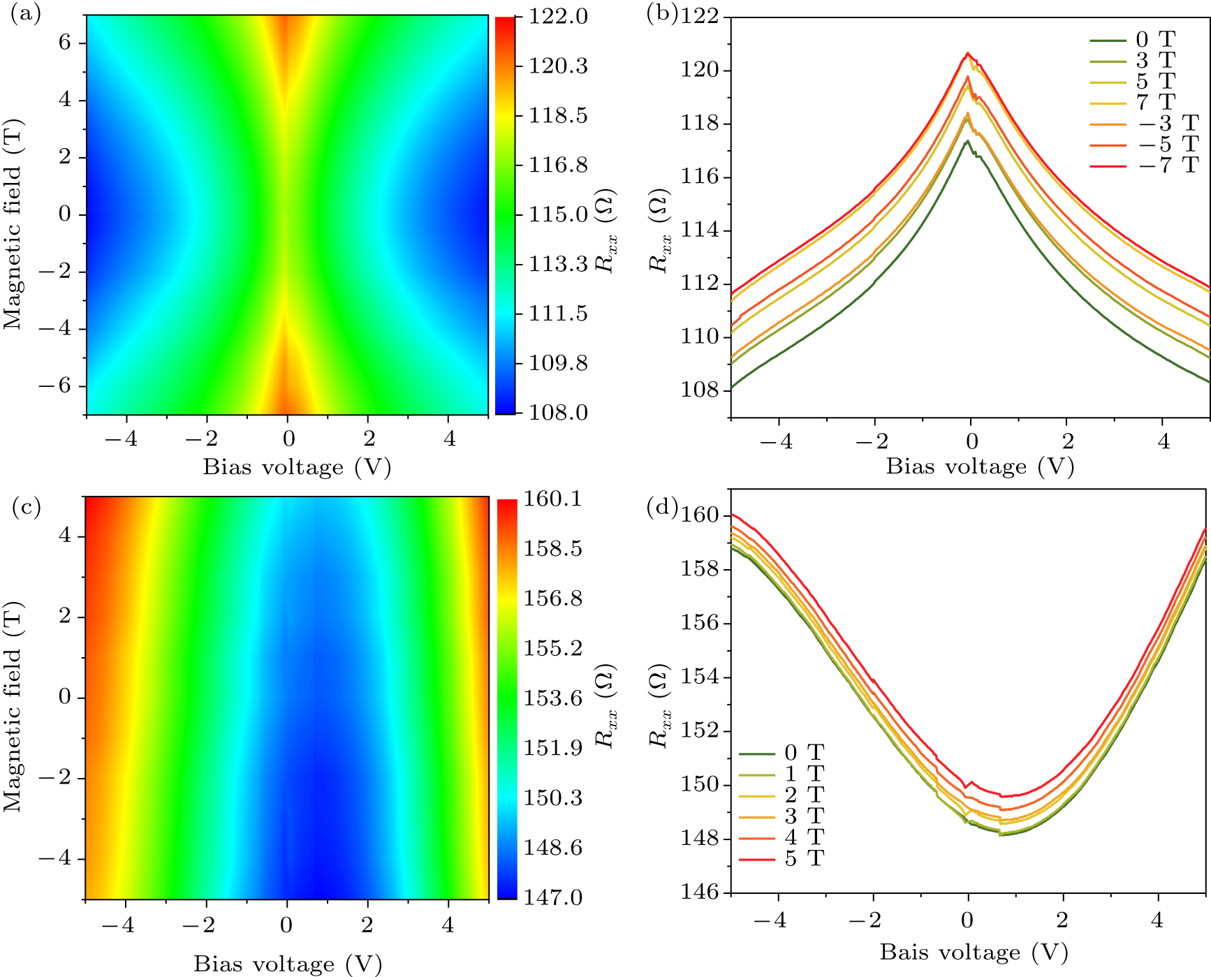
We studied the longitudinal magnetoresistance of the CrI3/graphene heterostructures as a function of external magnetic field, bias and gate voltages. All experimental results were obtained at 10 K. Ferromagnetic CrI3 leads to a magnetic proximity effect at the interface of CrI3 and graphene, which gives rise to a magnetoresistance effect. Figure 2(a) shows the color map of magnetoresistance as a function of magnetic field and bias at 10 K. The magnetoresistance increases with the increase of the external magnetic field, but decreases with increasing bias voltage. While the magnetoresistance of graphene shows a reverse behavior under bias voltage, which entirely differs from the magnetoresistance behaviors in the CrI3/graphene heterostructures (Figs. 2(c) and 2(d)). But the mechanism opposite magnetoresistance behaviors needs to be further studied.
Fig. 2. (a) Color map of magnetoresistance as a function of magnetic field and bias voltage in CrI3/graphene heterojunction at 10 K. (b) Selected resistance curves with bias voltage under different magnetic fields of (a). (c) Color map of magnetoresistance as a function of magnetic field and bias voltage in pristine graphene at 10 K. (d) Selected resistance curves with bias voltage under different magnetic fields of (c).
Figure 2(b) displays the magnetoresistance curves as a function of bias voltage under selected magnetic fields. The magnetoresistance change trend shows an even-symmetry behavior with magnetic field and bias voltage. When the magnetic fields increase from 0 to 7 T without applying a bias voltage, the magnetoresistance ratio reaches ∼ 2.8%, which is defined as (Rxx(H) – Rxx(0))/Rxx(0). The Lorentz force arising from the perpendicular out-of-plane magnetic field exerts a transverse force on the moving charge carriers in the xy direction and pushes them to the side of graphene, the carriers thus decrease in the xx direction, which gives rise to the increase of the resistance. In contrast, the bias voltage gives an electric force in the xx direction, which increases the carrier velocities, therefore, the resistance decreases as a function of the bias voltage. The resistance decreases from 116.9 Ω to 108.1 Ω as the bias voltage increase from 0 to ± 5 V, giving an approximately 7.5% reduction.
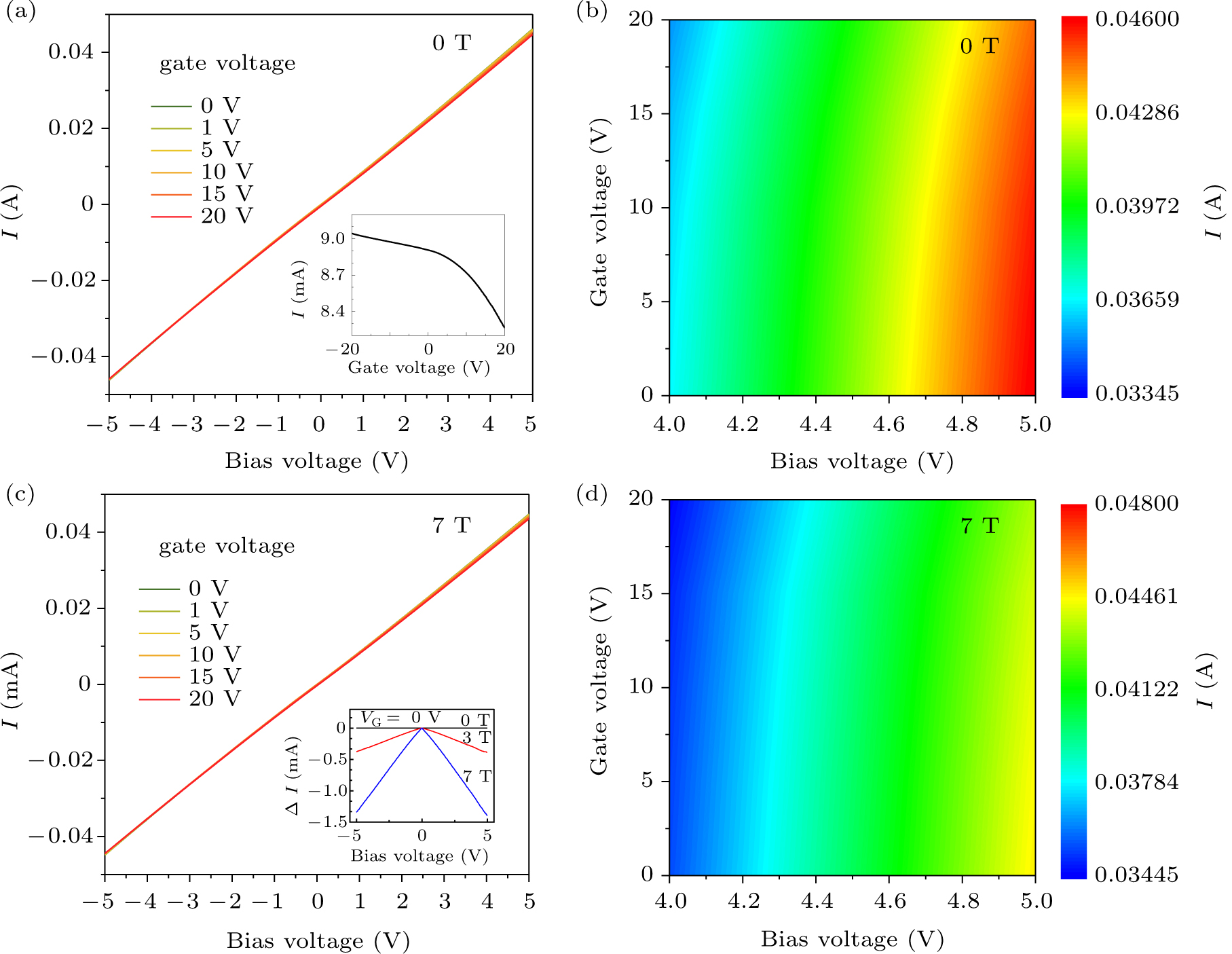
Figure 3 shows the I–V curves as a function of bias and gate voltage under external magnetic fields of 0 and 7 T, respectively. The I–V curves are nearly linear in CrI3/graphene heterostructures, indicating that the conductive behaviors are still preserved. Additionally, the color maps of enlarged I–V curves are shown in Figs. 3(b) and 3(d). As the gate voltage increases, the current of the CrI3/graphene heterostructures decreases under the same bias voltage. And the increasing magnetic field also leads to decreasing current. When the magnetic field is 0 T and the bias voltage is 4 V, the current under a gate voltage of 0 V is ∼ 36.6 mA, but the current decreases to 35.3 mA when the gate voltage increases to 20 V, giving rise to a decrease ratio of –3.6%. The I–V curve as a function of gate voltage also confirms that the current decreases with increasing positive gate voltage, indicating a p-type behavior, as shown in the inset in Fig. 3(a). Positive gate voltage results in a decrease of the carrier density and further induces a decreasing current. Alternatively, the magnetic field also induces the current decrease (Figs. 3(c) and 3(d)). The current decreases to 34.5 mA at 7 T compared with 35.3 mA at 0 T in the case of 4 V bias and 20 V gate voltage. Inset in Fig. 3(c) shows the decrease of current, Δ I, defined by Ixx(T) – Ixx(0), as a function of bias voltage under selected magnetic fields of 0, 3 T, and 7 T. With increasing magnetic field, the current decreases; and further decrease of current is induced at a higher bias voltage. These experimental results validate that the Lorentz force originating from the magnetic field reduces the current and results in the magnetoresistance behaviors.
Fig. 3. The I–V curves as a function of gate voltage at (a), (b) 0 and (c), (d) 7 T. (b), (d) Color maps of enlarged I–V curves, revealing that the current decreases with increasing gate voltage and external magnetic field. The insert in (a) is I–VG curve of graphene, indicating p-type behavior. The insert in (c) shows Δ I defined as Ixx (T) – Ixx(0), as a function of bias voltage under selected magnetic fields of 0, 3 T, and 7 T.
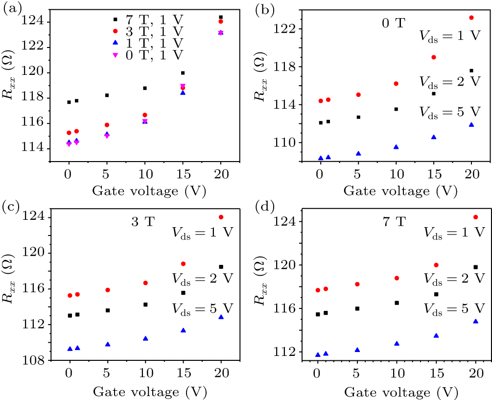
To understand the magnetoresistance behaviors of the heterostructures, we studied the magnetoresistance as a function of gate voltage. In a 0 or 1 T magnetic field, the resistance increases from ∼ 114.4 Ω to ∼ 123.2 Ω as the gate voltage increases from 0 to 20 V at a bias voltage of 1 V; and when the magnetic field is 3 T and 7 T, the resistance changes from ∼ 115.3 Ω and ∼ 117.7 Ω to ∼ 124.1 Ωand ∼ 124.4 Ω, respectively (Figs. 4(a)–4(d)). The magnetoresistance ratios are ∼ 2.9%, 0.8% and 0.09% without gate voltage under a 1 V bias voltage and magnetic fields of 1 T, 3 T and 7 T, respectively; while the magnetoresistance ratios decrease to ∼ 1%, 0.7% and 0 at a gate voltage 20 V. The resistance shows a nonlinear increase as a function of gate voltage. Figures 4(b)–4(d) show the resistance as a function of gate voltage at bias voltages of 1 V, 2 V and 5 V in a selected magnetic field of 0, 3 T and 7 T. Similar gate voltage control behaviors are observed at distinct bias voltage and magnetic field. Qualitatively, positive gate voltage leads to decreases of the carrier concentration, thus the resistance increases, but the mechanism is not clear at present and should be studied further.
Fig. 4. Magnetoresistance of CrI3-graphene heterostructure as a function of gate voltage. (a) Magnetoresistance as a function of gate voltage at 0, 1 T, 3 T and 7 T. (b)–(d) Magnetoresistance vs. gate voltage at a bias voltage of 1 V, 2 V and 5 V in a selected magnetic field of 0, 3 T and 7 T.
Conclusion
In summary, this work experimentally demonstrated a tunable magnetoresistance in CrI3/graphene heterostructures by bias and gate voltage, which provided plenty of opportunities toward novel spintronic and memory devices using 2D vdW materials. Electric-field control of magnetoresistance in CrI3/graphene ferromagnetic heterostructures opens the door to realizing in-memory computing to overcome the memory wall in the conventional von Neumann computing architecture.
... Controlling the spin degree of freedom is a vital foundation of spintronic devices and magnetic memory with ultralow energy consumption, ultrahigh speed and density in modern electronics. Graphene has provided a rich platform for exploiting spin controlling at the limit of single or few atomic layers,[1–4] which brokes the inherent cognition that two-dimensional monolayer could not stably exist at room temperature, which has exhibited plenty of unprecedented functions and unique properties, such as long spin lifetime, long spin transport distance and high carrier mobility,[5,6] allowing it to transmit and manipulate spin signals in complex multi-terminal device architectures.[7,8] This has enabled vast flexibility for creating graphene-based spintronic devices[9–12] and for cashing out values of graphene. Long-range ferromagnetic orders have recently been reported in diverse vdW ferromagnetic materials,[13–17] such as CrI3, Cr2Ge2Te6 and Fe3GeTe2.[18–22] This makes it possible to create a heterostructure comprising graphene and distinct two-dimensional (2D) vdW ferromagnetic materials to create spintronic devices with unique functions beyond the reach of isolated layered materials.[23–27] Magnetic proximity effect has been recently reported in CrBr3/graphene heterostructures, which show strong magnetic exchange leading to a significant Zeeman splitting field in graphene. ...
0
2004
0
2005
1
2018
... Controlling the spin degree of freedom is a vital foundation of spintronic devices and magnetic memory with ultralow energy consumption, ultrahigh speed and density in modern electronics. Graphene has provided a rich platform for exploiting spin controlling at the limit of single or few atomic layers,[1–4] which brokes the inherent cognition that two-dimensional monolayer could not stably exist at room temperature, which has exhibited plenty of unprecedented functions and unique properties, such as long spin lifetime, long spin transport distance and high carrier mobility,[5,6] allowing it to transmit and manipulate spin signals in complex multi-terminal device architectures.[7,8] This has enabled vast flexibility for creating graphene-based spintronic devices[9–12] and for cashing out values of graphene. Long-range ferromagnetic orders have recently been reported in diverse vdW ferromagnetic materials,[13–17] such as CrI3, Cr2Ge2Te6 and Fe3GeTe2.[18–22] This makes it possible to create a heterostructure comprising graphene and distinct two-dimensional (2D) vdW ferromagnetic materials to create spintronic devices with unique functions beyond the reach of isolated layered materials.[23–27] Magnetic proximity effect has been recently reported in CrBr3/graphene heterostructures, which show strong magnetic exchange leading to a significant Zeeman splitting field in graphene. ...
1
2016
... Controlling the spin degree of freedom is a vital foundation of spintronic devices and magnetic memory with ultralow energy consumption, ultrahigh speed and density in modern electronics. Graphene has provided a rich platform for exploiting spin controlling at the limit of single or few atomic layers,[1–4] which brokes the inherent cognition that two-dimensional monolayer could not stably exist at room temperature, which has exhibited plenty of unprecedented functions and unique properties, such as long spin lifetime, long spin transport distance and high carrier mobility,[5,6] allowing it to transmit and manipulate spin signals in complex multi-terminal device architectures.[7,8] This has enabled vast flexibility for creating graphene-based spintronic devices[9–12] and for cashing out values of graphene. Long-range ferromagnetic orders have recently been reported in diverse vdW ferromagnetic materials,[13–17] such as CrI3, Cr2Ge2Te6 and Fe3GeTe2.[18–22] This makes it possible to create a heterostructure comprising graphene and distinct two-dimensional (2D) vdW ferromagnetic materials to create spintronic devices with unique functions beyond the reach of isolated layered materials.[23–27] Magnetic proximity effect has been recently reported in CrBr3/graphene heterostructures, which show strong magnetic exchange leading to a significant Zeeman splitting field in graphene. ...
1
2015
... Controlling the spin degree of freedom is a vital foundation of spintronic devices and magnetic memory with ultralow energy consumption, ultrahigh speed and density in modern electronics. Graphene has provided a rich platform for exploiting spin controlling at the limit of single or few atomic layers,[1–4] which brokes the inherent cognition that two-dimensional monolayer could not stably exist at room temperature, which has exhibited plenty of unprecedented functions and unique properties, such as long spin lifetime, long spin transport distance and high carrier mobility,[5,6] allowing it to transmit and manipulate spin signals in complex multi-terminal device architectures.[7,8] This has enabled vast flexibility for creating graphene-based spintronic devices[9–12] and for cashing out values of graphene. Long-range ferromagnetic orders have recently been reported in diverse vdW ferromagnetic materials,[13–17] such as CrI3, Cr2Ge2Te6 and Fe3GeTe2.[18–22] This makes it possible to create a heterostructure comprising graphene and distinct two-dimensional (2D) vdW ferromagnetic materials to create spintronic devices with unique functions beyond the reach of isolated layered materials.[23–27] Magnetic proximity effect has been recently reported in CrBr3/graphene heterostructures, which show strong magnetic exchange leading to a significant Zeeman splitting field in graphene. ...
1
2019
... Controlling the spin degree of freedom is a vital foundation of spintronic devices and magnetic memory with ultralow energy consumption, ultrahigh speed and density in modern electronics. Graphene has provided a rich platform for exploiting spin controlling at the limit of single or few atomic layers,[1–4] which brokes the inherent cognition that two-dimensional monolayer could not stably exist at room temperature, which has exhibited plenty of unprecedented functions and unique properties, such as long spin lifetime, long spin transport distance and high carrier mobility,[5,6] allowing it to transmit and manipulate spin signals in complex multi-terminal device architectures.[7,8] This has enabled vast flexibility for creating graphene-based spintronic devices[9–12] and for cashing out values of graphene. Long-range ferromagnetic orders have recently been reported in diverse vdW ferromagnetic materials,[13–17] such as CrI3, Cr2Ge2Te6 and Fe3GeTe2.[18–22] This makes it possible to create a heterostructure comprising graphene and distinct two-dimensional (2D) vdW ferromagnetic materials to create spintronic devices with unique functions beyond the reach of isolated layered materials.[23–27] Magnetic proximity effect has been recently reported in CrBr3/graphene heterostructures, which show strong magnetic exchange leading to a significant Zeeman splitting field in graphene. ...
1
2015
... Controlling the spin degree of freedom is a vital foundation of spintronic devices and magnetic memory with ultralow energy consumption, ultrahigh speed and density in modern electronics. Graphene has provided a rich platform for exploiting spin controlling at the limit of single or few atomic layers,[1–4] which brokes the inherent cognition that two-dimensional monolayer could not stably exist at room temperature, which has exhibited plenty of unprecedented functions and unique properties, such as long spin lifetime, long spin transport distance and high carrier mobility,[5,6] allowing it to transmit and manipulate spin signals in complex multi-terminal device architectures.[7,8] This has enabled vast flexibility for creating graphene-based spintronic devices[9–12] and for cashing out values of graphene. Long-range ferromagnetic orders have recently been reported in diverse vdW ferromagnetic materials,[13–17] such as CrI3, Cr2Ge2Te6 and Fe3GeTe2.[18–22] This makes it possible to create a heterostructure comprising graphene and distinct two-dimensional (2D) vdW ferromagnetic materials to create spintronic devices with unique functions beyond the reach of isolated layered materials.[23–27] Magnetic proximity effect has been recently reported in CrBr3/graphene heterostructures, which show strong magnetic exchange leading to a significant Zeeman splitting field in graphene. ...
1
2009
... Controlling the spin degree of freedom is a vital foundation of spintronic devices and magnetic memory with ultralow energy consumption, ultrahigh speed and density in modern electronics. Graphene has provided a rich platform for exploiting spin controlling at the limit of single or few atomic layers,[1–4] which brokes the inherent cognition that two-dimensional monolayer could not stably exist at room temperature, which has exhibited plenty of unprecedented functions and unique properties, such as long spin lifetime, long spin transport distance and high carrier mobility,[5,6] allowing it to transmit and manipulate spin signals in complex multi-terminal device architectures.[7,8] This has enabled vast flexibility for creating graphene-based spintronic devices[9–12] and for cashing out values of graphene. Long-range ferromagnetic orders have recently been reported in diverse vdW ferromagnetic materials,[13–17] such as CrI3, Cr2Ge2Te6 and Fe3GeTe2.[18–22] This makes it possible to create a heterostructure comprising graphene and distinct two-dimensional (2D) vdW ferromagnetic materials to create spintronic devices with unique functions beyond the reach of isolated layered materials.[23–27] Magnetic proximity effect has been recently reported in CrBr3/graphene heterostructures, which show strong magnetic exchange leading to a significant Zeeman splitting field in graphene. ...
0
2018
0
2007
1
2017
... Controlling the spin degree of freedom is a vital foundation of spintronic devices and magnetic memory with ultralow energy consumption, ultrahigh speed and density in modern electronics. Graphene has provided a rich platform for exploiting spin controlling at the limit of single or few atomic layers,[1–4] which brokes the inherent cognition that two-dimensional monolayer could not stably exist at room temperature, which has exhibited plenty of unprecedented functions and unique properties, such as long spin lifetime, long spin transport distance and high carrier mobility,[5,6] allowing it to transmit and manipulate spin signals in complex multi-terminal device architectures.[7,8] This has enabled vast flexibility for creating graphene-based spintronic devices[9–12] and for cashing out values of graphene. Long-range ferromagnetic orders have recently been reported in diverse vdW ferromagnetic materials,[13–17] such as CrI3, Cr2Ge2Te6 and Fe3GeTe2.[18–22] This makes it possible to create a heterostructure comprising graphene and distinct two-dimensional (2D) vdW ferromagnetic materials to create spintronic devices with unique functions beyond the reach of isolated layered materials.[23–27] Magnetic proximity effect has been recently reported in CrBr3/graphene heterostructures, which show strong magnetic exchange leading to a significant Zeeman splitting field in graphene. ...
1
2019
... Controlling the spin degree of freedom is a vital foundation of spintronic devices and magnetic memory with ultralow energy consumption, ultrahigh speed and density in modern electronics. Graphene has provided a rich platform for exploiting spin controlling at the limit of single or few atomic layers,[1–4] which brokes the inherent cognition that two-dimensional monolayer could not stably exist at room temperature, which has exhibited plenty of unprecedented functions and unique properties, such as long spin lifetime, long spin transport distance and high carrier mobility,[5,6] allowing it to transmit and manipulate spin signals in complex multi-terminal device architectures.[7,8] This has enabled vast flexibility for creating graphene-based spintronic devices[9–12] and for cashing out values of graphene. Long-range ferromagnetic orders have recently been reported in diverse vdW ferromagnetic materials,[13–17] such as CrI3, Cr2Ge2Te6 and Fe3GeTe2.[18–22] This makes it possible to create a heterostructure comprising graphene and distinct two-dimensional (2D) vdW ferromagnetic materials to create spintronic devices with unique functions beyond the reach of isolated layered materials.[23–27] Magnetic proximity effect has been recently reported in CrBr3/graphene heterostructures, which show strong magnetic exchange leading to a significant Zeeman splitting field in graphene. ...
0
2017
0
2017
0
2016
1
2016
... Controlling the spin degree of freedom is a vital foundation of spintronic devices and magnetic memory with ultralow energy consumption, ultrahigh speed and density in modern electronics. Graphene has provided a rich platform for exploiting spin controlling at the limit of single or few atomic layers,[1–4] which brokes the inherent cognition that two-dimensional monolayer could not stably exist at room temperature, which has exhibited plenty of unprecedented functions and unique properties, such as long spin lifetime, long spin transport distance and high carrier mobility,[5,6] allowing it to transmit and manipulate spin signals in complex multi-terminal device architectures.[7,8] This has enabled vast flexibility for creating graphene-based spintronic devices[9–12] and for cashing out values of graphene. Long-range ferromagnetic orders have recently been reported in diverse vdW ferromagnetic materials,[13–17] such as CrI3, Cr2Ge2Te6 and Fe3GeTe2.[18–22] This makes it possible to create a heterostructure comprising graphene and distinct two-dimensional (2D) vdW ferromagnetic materials to create spintronic devices with unique functions beyond the reach of isolated layered materials.[23–27] Magnetic proximity effect has been recently reported in CrBr3/graphene heterostructures, which show strong magnetic exchange leading to a significant Zeeman splitting field in graphene. ...
1
2019
... Controlling the spin degree of freedom is a vital foundation of spintronic devices and magnetic memory with ultralow energy consumption, ultrahigh speed and density in modern electronics. Graphene has provided a rich platform for exploiting spin controlling at the limit of single or few atomic layers,[1–4] which brokes the inherent cognition that two-dimensional monolayer could not stably exist at room temperature, which has exhibited plenty of unprecedented functions and unique properties, such as long spin lifetime, long spin transport distance and high carrier mobility,[5,6] allowing it to transmit and manipulate spin signals in complex multi-terminal device architectures.[7,8] This has enabled vast flexibility for creating graphene-based spintronic devices[9–12] and for cashing out values of graphene. Long-range ferromagnetic orders have recently been reported in diverse vdW ferromagnetic materials,[13–17] such as CrI3, Cr2Ge2Te6 and Fe3GeTe2.[18–22] This makes it possible to create a heterostructure comprising graphene and distinct two-dimensional (2D) vdW ferromagnetic materials to create spintronic devices with unique functions beyond the reach of isolated layered materials.[23–27] Magnetic proximity effect has been recently reported in CrBr3/graphene heterostructures, which show strong magnetic exchange leading to a significant Zeeman splitting field in graphene. ...
0
2020
0
2020
0
2020
1
2020
... Controlling the spin degree of freedom is a vital foundation of spintronic devices and magnetic memory with ultralow energy consumption, ultrahigh speed and density in modern electronics. Graphene has provided a rich platform for exploiting spin controlling at the limit of single or few atomic layers,[1–4] which brokes the inherent cognition that two-dimensional monolayer could not stably exist at room temperature, which has exhibited plenty of unprecedented functions and unique properties, such as long spin lifetime, long spin transport distance and high carrier mobility,[5,6] allowing it to transmit and manipulate spin signals in complex multi-terminal device architectures.[7,8] This has enabled vast flexibility for creating graphene-based spintronic devices[9–12] and for cashing out values of graphene. Long-range ferromagnetic orders have recently been reported in diverse vdW ferromagnetic materials,[13–17] such as CrI3, Cr2Ge2Te6 and Fe3GeTe2.[18–22] This makes it possible to create a heterostructure comprising graphene and distinct two-dimensional (2D) vdW ferromagnetic materials to create spintronic devices with unique functions beyond the reach of isolated layered materials.[23–27] Magnetic proximity effect has been recently reported in CrBr3/graphene heterostructures, which show strong magnetic exchange leading to a significant Zeeman splitting field in graphene. ...
0
2020
0
2020
0
2007
1
1990
... Controlling the spin degree of freedom is a vital foundation of spintronic devices and magnetic memory with ultralow energy consumption, ultrahigh speed and density in modern electronics. Graphene has provided a rich platform for exploiting spin controlling at the limit of single or few atomic layers,[1–4] which brokes the inherent cognition that two-dimensional monolayer could not stably exist at room temperature, which has exhibited plenty of unprecedented functions and unique properties, such as long spin lifetime, long spin transport distance and high carrier mobility,[5,6] allowing it to transmit and manipulate spin signals in complex multi-terminal device architectures.[7,8] This has enabled vast flexibility for creating graphene-based spintronic devices[9–12] and for cashing out values of graphene. Long-range ferromagnetic orders have recently been reported in diverse vdW ferromagnetic materials,[13–17] such as CrI3, Cr2Ge2Te6 and Fe3GeTe2.[18–22] This makes it possible to create a heterostructure comprising graphene and distinct two-dimensional (2D) vdW ferromagnetic materials to create spintronic devices with unique functions beyond the reach of isolated layered materials.[23–27] Magnetic proximity effect has been recently reported in CrBr3/graphene heterostructures, which show strong magnetic exchange leading to a significant Zeeman splitting field in graphene. ...
1
2017
... Here, we demonstrate a longitudinal magnetoresistance behavior with increasing external magnetic field in CrI3/graphene heterostructures. The magnetoresistance ratio is ∼ 2.8%. The magnetoresistance can be tuned by bias and gate voltage. With increasing bias voltage, the magnetoresistance decreases and the current increases; in contrast, a positive gate voltage decreases the magnetoresistance. A typical CrI3/graphene vdW heterostructure for electrical transport measurement is shown in Fig. 1(a). The CrI3 multilayers exfoliated from crystals by PDMS were transferred onto graphene. CrI3 is an Ising ferromagnet with out-of-plane spin orientation, showing strong out-of-plane magnetic anisotropy. The CrI3 monolayer exhibits ferromagnetism, and interlayer antiferromagnetic coupling leads to an antiferromagnetic arrangement in CrI3 bilayers.[28] The magnetism can be electrically controlled in CrI3 mono- and bi-layers through the magnetoelectric coupling effect.[29] The interfacial exchange coupling at the interface of CrI3 and graphene can significantly influence the electronic and optoelectronic properties of the layered crystals.[30–33] This study provides a platform for fundamental physics studies toward the next-generation 2D spin logic and memory devices. ...
1
2018
... Here, we demonstrate a longitudinal magnetoresistance behavior with increasing external magnetic field in CrI3/graphene heterostructures. The magnetoresistance ratio is ∼ 2.8%. The magnetoresistance can be tuned by bias and gate voltage. With increasing bias voltage, the magnetoresistance decreases and the current increases; in contrast, a positive gate voltage decreases the magnetoresistance. A typical CrI3/graphene vdW heterostructure for electrical transport measurement is shown in Fig. 1(a). The CrI3 multilayers exfoliated from crystals by PDMS were transferred onto graphene. CrI3 is an Ising ferromagnet with out-of-plane spin orientation, showing strong out-of-plane magnetic anisotropy. The CrI3 monolayer exhibits ferromagnetism, and interlayer antiferromagnetic coupling leads to an antiferromagnetic arrangement in CrI3 bilayers.[28] The magnetism can be electrically controlled in CrI3 mono- and bi-layers through the magnetoelectric coupling effect.[29] The interfacial exchange coupling at the interface of CrI3 and graphene can significantly influence the electronic and optoelectronic properties of the layered crystals.[30–33] This study provides a platform for fundamental physics studies toward the next-generation 2D spin logic and memory devices. ...
1
2017
... Here, we demonstrate a longitudinal magnetoresistance behavior with increasing external magnetic field in CrI3/graphene heterostructures. The magnetoresistance ratio is ∼ 2.8%. The magnetoresistance can be tuned by bias and gate voltage. With increasing bias voltage, the magnetoresistance decreases and the current increases; in contrast, a positive gate voltage decreases the magnetoresistance. A typical CrI3/graphene vdW heterostructure for electrical transport measurement is shown in Fig. 1(a). The CrI3 multilayers exfoliated from crystals by PDMS were transferred onto graphene. CrI3 is an Ising ferromagnet with out-of-plane spin orientation, showing strong out-of-plane magnetic anisotropy. The CrI3 monolayer exhibits ferromagnetism, and interlayer antiferromagnetic coupling leads to an antiferromagnetic arrangement in CrI3 bilayers.[28] The magnetism can be electrically controlled in CrI3 mono- and bi-layers through the magnetoelectric coupling effect.[29] The interfacial exchange coupling at the interface of CrI3 and graphene can significantly influence the electronic and optoelectronic properties of the layered crystals.[30–33] This study provides a platform for fundamental physics studies toward the next-generation 2D spin logic and memory devices. ...
0
2017
0
2018
1
2019
... Here, we demonstrate a longitudinal magnetoresistance behavior with increasing external magnetic field in CrI3/graphene heterostructures. The magnetoresistance ratio is ∼ 2.8%. The magnetoresistance can be tuned by bias and gate voltage. With increasing bias voltage, the magnetoresistance decreases and the current increases; in contrast, a positive gate voltage decreases the magnetoresistance. A typical CrI3/graphene vdW heterostructure for electrical transport measurement is shown in Fig. 1(a). The CrI3 multilayers exfoliated from crystals by PDMS were transferred onto graphene. CrI3 is an Ising ferromagnet with out-of-plane spin orientation, showing strong out-of-plane magnetic anisotropy. The CrI3 monolayer exhibits ferromagnetism, and interlayer antiferromagnetic coupling leads to an antiferromagnetic arrangement in CrI3 bilayers.[28] The magnetism can be electrically controlled in CrI3 mono- and bi-layers through the magnetoelectric coupling effect.[29] The interfacial exchange coupling at the interface of CrI3 and graphene can significantly influence the electronic and optoelectronic properties of the layered crystals.[30–33] This study provides a platform for fundamental physics studies toward the next-generation 2D spin logic and memory devices. ...