Growth and physical characterization of high resistivity Fe: β-Ga2O3 crystals
Zhang Hao1, Tang Hui-Li1, †, He Nuo-Tian1, Zhu Zhi-Chao2, Chen Jia-Wen1, Liu Bo1, Xu Jun1, 3
MOE Key Laboratory of Advanced Micro-Structured Materials, School of Physics Science and Engineering, Institute for Advanced Study, Tongji University, Shanghai 200092, China
School of Chemical Science and Engineering, Tongji University, Shanghai 200092, China
Shanghai Engineering Research Center for Sapphire Crystals, Shanghai 201899, China


† Corresponding author. E-mail: tanghl@tongji.edu.cn

Project supported by the Scientific and Innovative Action Plan of Shanghai, China (Grant No. 18511110502) and Equipment Pre-research Fund Key Project, China (Grant No. 6140922010601).

Abstract

High quality 0.02 mol%, 0.05 mol%, and 0.08 mol% Fe: β-Ga2O3 single crystals were grown by the floating zone method. The crystal structure, optical, electrical, and thermal properties were measured and discussed. Fe: β-Ga2O3 single crystals showed transmittance of higher than 80% in the near infrared region. With the increase of the Fe doping concentration, the optical bandgaps reduced and room temperature resistivity increased. The resistivity of 0.08 mol% Fe: β-Ga2O3 crystal reached to 3.63 × 10¹¹ Ω ⋅cm. The high resistivity Fe: β-Ga2O3 single crystals could be applied as the substrate for the high-power field effect transistors (FETs).

1. Introduction

The β-gallium oxide (β-Ga2O3) crystal has become an increasingly attractive semiconductor for the potential applications in the fields of high-power devices, solar blind ultraviolet photodetectors, and Schottky x-ray detectors[13] due to its outstanding material properties. Unintentionally-doped β-Ga2O3 has a bandgap of 4.5–4.9 eV[46] with a theoretical breakdown electric field of 8 MV/cm, which is two times larger than those of SiC and GaN.[7,8] Baliga’s figure of merit (BFOM) is 3214 which is only lower than that of diamond. Gallium oxide commonly has five polymorphs named as α, β, γ, δ, and ε. Among them, β-Ga2O3 is the most stable crystal structure.[9] High crystalline quality β-Ga2O3 bulk crystal can be grown by the melt-growth techniques such as Czochralski (CZ), edge-defined film-fed growth (EFG), and floating zone (FZ) method.[1012] With the development of β-Ga2O3 devices, the high resistance β-Ga2O3 substrate is needed to fabricate high-power field effect transistors to ensure lower leakage current.[1315] However, unintentionally-doped β-Ga2O3 usually exhibits n-type due to the residual impurities in raw materials such as Si, Sn, and Ge.[16] The electron concentration and resistivity of unintentionally-doped β-Ga2O3 are typically about 1017 cm−3 and 10−1 Ω ⋅cm, respectively.[1720] Doping deep acceptors is needed to compensate the free carriers to achieve semi-insulating (SI) β-Ga2O3.

Currently, β-Ga2O3 can be made SI by doping Fe.[2123] The Fe ion acts as deep acceptors in β-Ga2O3 and pins the Fermi level away from the conduction band (CB). By thermoluminescence (TL) spectroscopy, an additional defect center with an activation energy of 0.62 eV was introduced in Fe: β-Ga2O3 with the resistivity of 5.10× 10⁶ Ω ⋅cm.[24] An acceptor energy of 0.86 eV was tested by the high temperature Hall effect measurement in the conduction band with Fe doping concentration of 8× 1017 cm−3.[25] Based on first principles study, the bandgap of β-Ga2O3 reduced to 3.30 eV by doping Fe.[26] These results show that the defect energy may have relationship with the Fe doping concentration and influence the physical characterization of high resistivity Fe: β-Ga2O3 crystal.

In this paper, high resistivity Fe: β-Ga2O3 single crystals were grown by the FZ technique. The optical, electrical, and thermal properties of the as-grown crystals have been studied, which would provide basic performance parameters for the device fabrications.

2. Experimental methods

The 0.02 mol%, 0.05 mol%, and 0.08 mol% Fe: β-Ga2O3 single crystals were grown by the FZ method. Feed rods were prepared with gallium oxide powder (purity 99.9999%) and Fe2O3 powder (purity 99.99%). The rods were shaped by a cold press of 50 MPa for 20 min and then sintered at 1500 °C for 24 h in the air atmosphere. Crystal growth was carried out by advanced four halogen lamp floating zone furnace (Quantum De-sign-IRF01-001-00). The crystal growth rate was 5 mm/h with a rotation speed of 8 rpm in the air flow atmosphere along the [010] direction.

To analyze the single crystal structure and quality, the x-ray powder diffraction and x-ray diffraction rocking curve were tested by a Bruker D8 ADVANCE diffractometer. The optical transmission spectra were measured by an UV–VIS–NIR spectrophotometer (Varian Cary 5000). The room temperature current–voltage (IV) curves and the temperature dependence resistivity were obtained by a Keithley 4200 semiconductor characterization system and an Agilent 6517B megger. The specific heat and thermal diffusivity were tested by a DSC 8000 differential scanning calorimeter and a LFA467 Hyper Flash conductometer. The samples were cut along the (100) plane and double-sided polished by chemical mechanical polishing.

3. Results and discussion
3.1. Structure characterizations

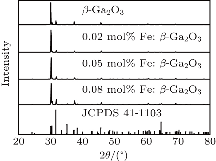
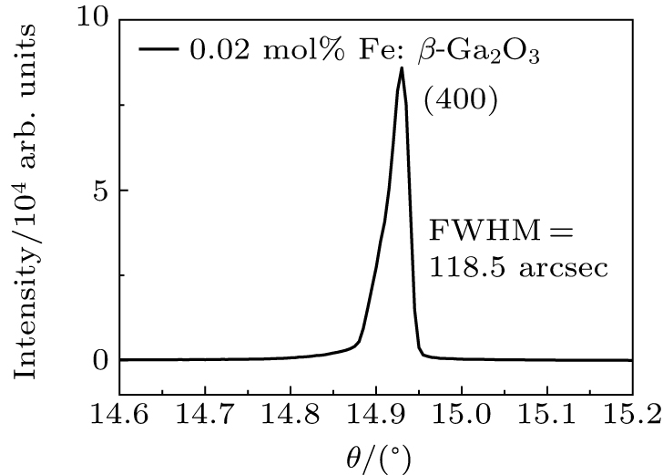
The as-grown Fe: β-Ga2O3 crystals are brown, transparent without cracks, as shown in Fig. 1. The diameter of 0.02 mol% Fe: β-Ga2O3 crystal is about 6 mm, the length is about 20 mm, and the analysis of GDMS shows that the actual doping concentration of Fe ion is 17 μg/g. The colors of the crystals become deeper with the increase of Fe doping concentration. Figure 2 shows the x-ray diffraction (XRD) patterns of the as-grown crystals. All the diffraction peaks could be indexed in monoclinic phase β-Ga2O3 (PDF #41-1103), indicating that the dopant did not change the crystal structure. The unit cell parameters of 0.02 mol% Fe: β-Ga2O3 were calculated as a = 12.1974 Å, b = 3.0355 Å, c = 5.7861 Å and β = 103.88°, and the unit cell parameters of unintentionally-doped β-Ga2O3 were calculated as a = 12.1797 Å, b = 3.0319 Å, c = 5.7852 Å and β = 103.38° The ionic radius of Fe2+/3+ is bigger than that of Ga3+, and thus the unit cell parameters increase after doping Fe. The crystalline quality was evaluated by high-resolution x-ray diffraction. The x-ray diffraction rocking curve of 0.02 mol% Fe: β-Ga2O3 wafer is shown in Fig. 3. The rocking curve is symmetrical with the full-width at half-maximum of 118.5 arcsec, indicating that the crystal has a good crystal quality without sub-grain boundaries.

Fig. 1. The 0.02 mol% Fe: β-Ga2O3 single crystal.
Fig. 2. The XRD patterns of β-Ga2O3 and Fe: β-Ga2O3 crystals.
Fig. 3. XRD rocking curve of 0.02 mol% Fe: β-Ga2O3 wafer.
3.2. Optical properties of Fe: β-Ga2O3

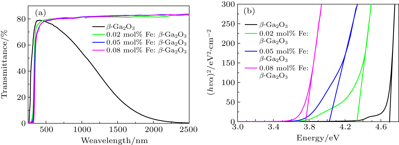
Figure 4(a) shows the optical transmission spectra of 0.02 mol%, 0.05 mol%, and 0.08 mol% Fe: β-Ga2O3 wafers with the thickness of 2 mm. Fe: β-Ga2O3 single crystals showed transmittance of higher than 80% in the near infrared region while the transmittance of unintentionally-doped β-Ga2O3 fell rapidly with the increase of wavelength. Low transmittance in the near infrared region could be ascribed to the plasma reflection of conduction electrons.[16] It can be seen that Fe: β-Ga2O3 crystals have high resistivity. The absorption edge of unintentionally-doped β-Ga2O3 was determined to be 264 nm. The absorption edges of 0.02 mol%, 0.05 mol%, and 0.08 mol% Fe: β-Ga2O3 increased to 288 nm, 309 nm, and 327 nm, respectively.

Fig. 4. Room-temperature optical transmission spectra (a) and absorption edges (b) of 0.02 mol%, 0.05 mol%, and 0.08 mol% Fe-doped β-Ga2O3 crystals.

The optical bandgap energy can be obtained by plotting (αhν)2 against , where α is the absorption coefficient and is the photon energy.[24,27] As shown in Fig. 4(b), the optical bandgaps reduced with the increase of the Fe doping concentration. In the cases of pure, 0.02 mol%, 0.05 mol%, and 0.08 mol% Fe: β-Ga2O3, the optical bandgaps were 4.695 eV, 4.338 eV, 4.044 eV, and 3.760 eV, respectively. First principles study on the electrical properties of Fe: β-Ga2O3 found a significant decrease in the optical bandgap from 4.80 eV to 3.30 eV,[26] which is consistent with our results. The bandgap narrowing occurs in the Cr-doped SI GaAs samples due to the screening of the electron–hole interaction caused by the presence of both Cr2+ and Cr3+ states of chromium.[28] For Fe-doped SI InP samples, the Fe dopant gives rise to the bandgap narrowing.[29] The relationship between the concentration of the Fe dopant and the optical bandgap of Fe: β-Ga2O3 is shown in Table 1. The concentration of the Fe dopant is inversely proportional to the optical bandgap. It may be that the defect energy caused by doping Fe[2325] broadens with the increase of the Fe doping concentration.

Table 1.

Influences of the Fe dopant on the optical bandgap and resistivity.

.
3.3. Electrical properties of Fe: β-Ga2O3

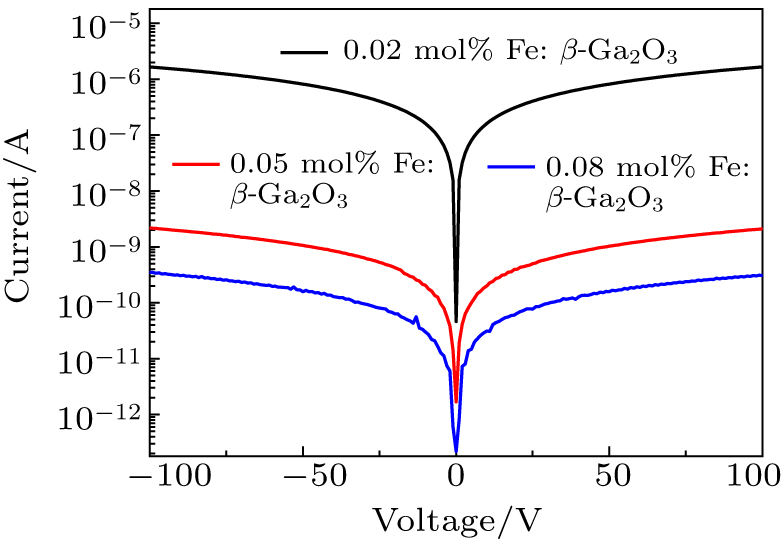
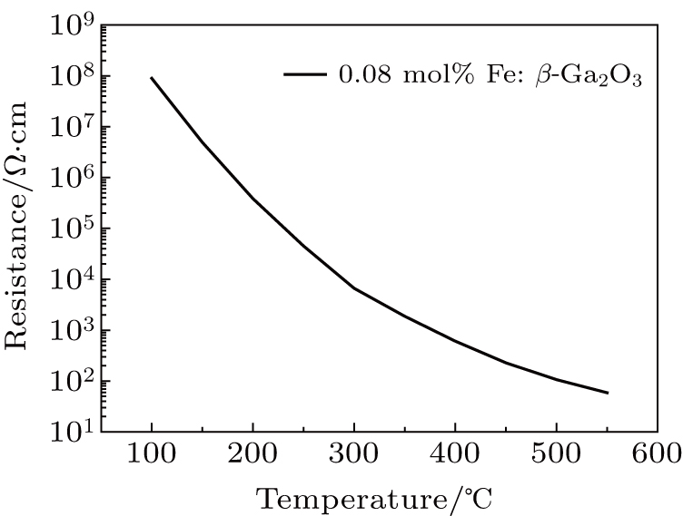
The root mean square roughness (RMS) of the polished samples is about 0.5 nm in the area of 7 μm × 7 μm tested by atomic force microscopy. The samples were cleaned by acetone and Ti/Au (20 nm/50 nm) electrodes were deposited by electron-beam evaporation with an area of 4 mm × 4 mm. In order to obtain Ohmic contact between Ti and Fe: β-Ga2O3, a rapid thermal annealing at 850 °C for 30 s in the nitrogen atmosphere was performed. Figure 5 shows the current–voltage (IV) curves of Fe: β-Ga2O3, which exhibited a good Ohmic contact behavior. From Table 1, it can be seen that the resistivity increased and the increasing trend slowed down with the increase of the Fe doping concentration and there was a negative correlation between the resistivity and the optical bandgap. The resistivity of unintentionally-doped β-Ga2O3 was measured to be 2.40× 10⁻¹ Ω ⋅cm at room temperature, while the resistivity of 0.02 mol%, 0.05 mol%, and 0.08 mol% Fe: β-Ga2O3 reached to 1.89× 10⁸ Ω ⋅cm, 8.47× 10¹⁰ Ω ⋅cm, and 3.63× 10¹¹ Ω ⋅cm, respectively. Temperature-dependent resistivity of 0.08 mol% Fe: β-Ga2O3 was tested from 100 °C to 550 °C. As shown in Fig. 6, the resistivity was 8.92× 10⁷ Ω ⋅cm at 100 °C, and decreased rapidly to 59 Ω ⋅cm when the temperature raised up to 550 °C. It might be that the Fe ion acts as acceptors in Fe: β-Ga2O3 single crystals and the captured electrons would be released with the increase of temperature.[30]

Fig. 5. The IV curves of 0.02 mol%, 0.05 mol%, and 0.08 mol% Fe: β-Ga2O3 crystals.
Fig. 6. Temperature-dependent resistivity of 0.08 mol% Fe: β-Ga2O3 crystal from 100 °C to 550 °C.
3.4. Thermal conductivity of Fe: β-Ga2O3

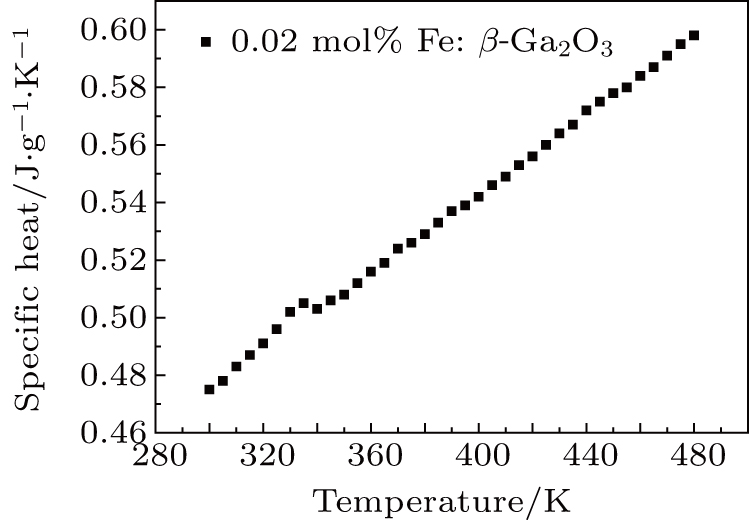
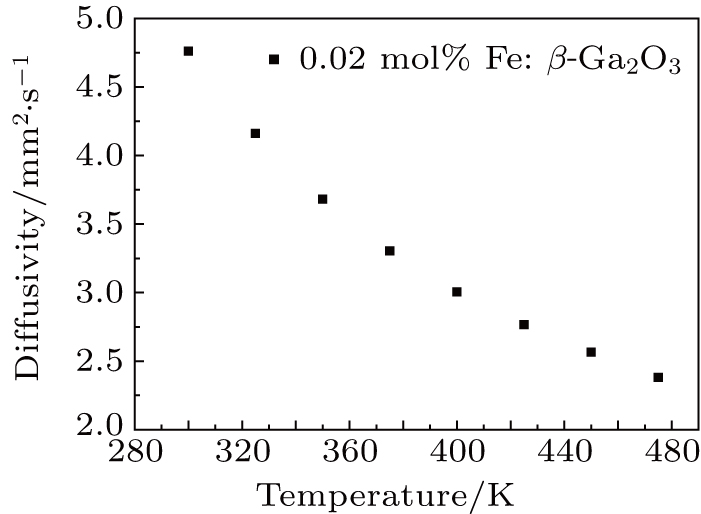
The thermal conductivity of the substrate plays an important role in the β-Ga2O3 power devices. 0.02 mol% Fe: β-Ga2O3 crystal was cut into 4 mm × 3 mm × 1 mm to test the specific heat. Figure 7 exhibits that the specific heat improved with the increase of temperature. The specific heat increased from 0.475 J/g⋅K at 300 K to 0.598 J/g⋅K at 475 K. Figure 8 presents the thermal diffusivity of 0.02 mol% Fe: β-Ga2O3 along the [100] direction. The thermal diffusivity decreased with the increase of temperature, which was 4.761 mm2/s at 300 K and 2.381 mm2/s at 475 K. The density of Fe: β-Ga2O3 was 5.651 g/cm3 at room temperature measured by the drainage method. The thermal conductivity was calculated to be 12.780 W/m⋅K at room temperature, a little smaller than the reported result of 16 W/m⋅K calculated for β-Ga2O3 by the first law at 300 K,[31] but larger than 10.9 ± 1 W/m⋅K of the Sn: β-Ga2O3 at room temperature.[32] It was reported that the phonon-point-defect scattering would reduce the thermal conductivity.[33] The reason behind the discrepancies in the reported values of thermal conductivity could be due to the increase of phonon-point-defect scattering by doping Fe ion.

Fig. 7. Temperature-dependent specific heat of 0.02 mol% Fe: β-Ga2O3 crystal.
Fig. 8. Temperature-dependent thermal diffusivity of 0.02 mol% Fe: β-Ga2O3 crystal along the [100] direction.
4. Conclusion

Fe: β-Ga2O3 crystals with different doping concentrations were grown by the FZ method. With the increase of the Fe doping concentration to 0.08 mol%, the optical bandgap reduces to 3.760 eV. For the unintentionally-doped β-Ga2O3 crystal, the optical bandgap is 4.695 eV. Fe: β-Ga2O3 crystals have high resistivity at room temperature. The room temperature resistivity of 0.08 mol% Fe: β-Ga2O3 crystal is 3.63 × 10¹¹ Ω ⋅cm, and the resistivity reduces rapidly to 59 Ω ⋅ cm when the temperature raises up to 550 °C. The thermal conductivity of the 0.02 mol% Fe: β-Ga2O3 crystal is 12.780 W/m⋅K at room temperature, slightly lower than the reported result of β-Ga2O3 crystal. Fe: β-Ga2O3 crystal is a good candidate for high-power devices.

Reference
[1] Higashiwaki M Sasaki K Murakami H Kumagai Y Koukitu A Kuramata A Masui T Yamakoshi S 2016 Semicond. Sci. Tech. 31 034001
[2] Oh S Jung Y Mastro M A Hite J K Eddy C R Kim J 2015 Opt. Express 23 28300
[3] Lu X Zhou L Chen L Ouyang X Liu B Xu J Tang H 2018 Appl. Phys. Lett. 112 103502
[4] Tippins H H 1965 Phys. Rev. 140 A316
[5] Stepanov S Nikolaev V Bougrov V Romanov A 2016 Rev. Adv. Mater. Sci. 44 63
[6] He H Orlando R Blanco M A Pandey R Amzallag E Baraille I Rérat M 2006 Phys. Rev. 74 195123
[7] Higashiwaki M Sasaki K Kamimura T Hoi Wong M Krishnamurthy D Kuramata A Masui T Yamakoshi S 2013 Appl. Phys. Lett. 103 123511
[8] Yan X Esqueda I S Ma J Tice J Wang H 2018 Appl. Phys. Lett. 112 032101
[9] Roy R Hill V G Osborn E F 1952 J. Am. Chem. Soc. 74 719
[10] Galazka Z Uecker R Irmscher K Albrecht M Klimm D Pietsch M Brützam M Bertram R Ganschow S Fornari R 2010 Cryst. Res. Technol. 45 1229
[11] Víllora E G Shimamura K Yoshikawa Y Aoki K Ichinose N 2004 J. Cryst. Growth 270 420
[12] Kuramata A Koshi K Watanabe S Yamaoka Y Masui T Yamakoshi S 2016 Jpn. J. Appl. Phys. 55 1202A2
[13] Zhang Z Farzana E Arehart A R Ringel S A 2016 Appl. Phys. Lett. 108 052105
[14] Green A J Chabak K D Heller E R Fitch R C Baldini M Fiedler A Irmscher K Wagner G Galazka Z Tetlak S E Crespo A 2016 IEEE Electr. Device Lett. 37 902
[15] Wong M H Sasaki K Kuramata A Yamakoshi S Higashiwaki M 2015 IEEE Electr. Device Lett. 37 212
[16] Tang H He N Zhang H Liu B Zhu Z Xu M Chen L Liu J Ouyang X Xu J 2020 CrystEngComm 22 924
[17] Onuma T Fujioka S Yamaguchi T Higashiwaki M Sasaki K Masui T Honda T 2013 Appl. Phys. Lett. 103 041910
[18] Irmscher K Galazka Z Pietsch M Uecker R Fornari R 2011 J. Appl. Phys. 110 063720
[19] Galazka Z Irmscher K Uecker R Bertram R Pietsch M Kwasniewski A Naumann M Schulz T Schewski R Klimm D Bickermann M 2014 J. Cryst. Growth 404 184
[20] Suzuki N Ohira S Tanaka M Sugawara T Nakajima K Shishido T 2007 Phys. Status Solidi 4 2310
[21] Wong M H Sasaki K Kuramata A Yamakoshi S Higashiwaki M 2015 Appl. Phys. Lett. 106 032105
[22] Polyakov A Y Smirnov N B Shchemerov I V Pearton S J Ren F Chernykh A V Kochkova A I 2018 Appl. Phys. Lett. 113 142102
[23] Ingebrigtsen M E Varley J B Kuznetsov A Y Svensson B G Alfieri G Mihaila A Badstübner U Vines L 2018 Appl. Phys. Lett. 112 042104
[24] Islam M M Rana D Hernandez A Haseman M Selim F A 2019 J. Appl. Phys. 125 055701
[25] Neal A T Mou S Rafique S Rafique S Zhao H Ahmadi E Speck J S Stevens K T Blevins J D Thomson D B Moser N Chabak K D 2018 Appl. Phys. Lett. 113 062101
[26] He H Li W Xing H Z Liang E J 2012 Adv. Mater. Res. 535 36
[27] Ricci F Boschi F Baraldi A Filippetti A Higashiwaki M Kuramata A Fiorentini V Fornari and R 2016 J. Phys.: Condens. Matter 28 224005
[28] Hrivnák L 1987 J. Appl. Phys. 62 3228
[29] Fornari R Kumar J 1990 Appl. Phys. Lett. 56 638
[30] Lenyk C A Gustafson T D Halliburton L E Giles N C 2019 J. Appl. Phys. 126 245701
[31] Santia M D Tandon N Albrecht J D 2015 Appl. Phys. Lett. 107 041907
[32] Guo Z Verma A Wu X Sun F Hickman A Masui T Kuramata A Higashiwaki M Jena D Luo T 2015 Appl. Phys. Lett. 106 111909
[33] Slomski M Blumenschein N Paskov P P Muth J F Paskova T 2017 J. Appl. Phys. 121 235104