An artificial synapse by superlattice-like phase-change material for low-power brain-inspired computing
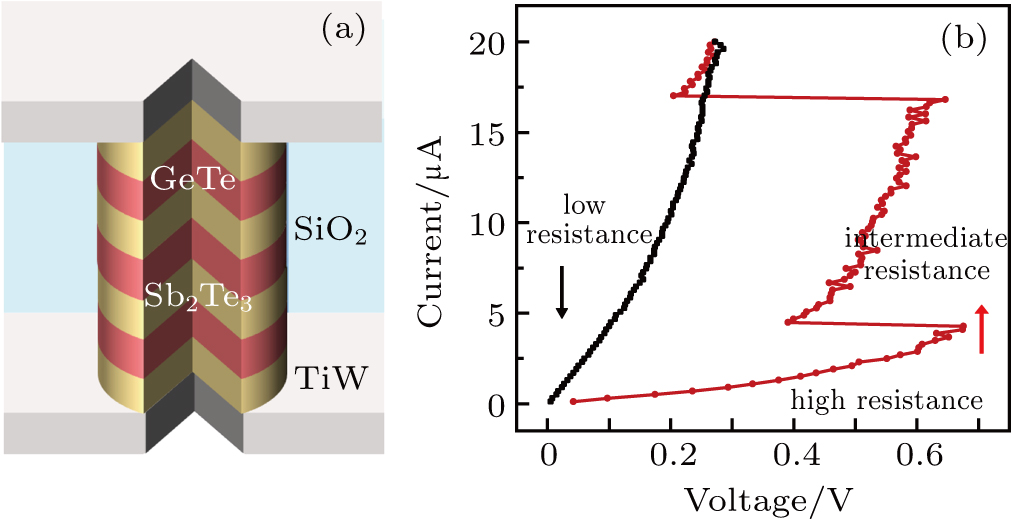
Device fabrication and electrical characteristics. (a) Schematic of the via-hole GeTe/Sb2Te3 SLL PCM device. The total thickness of the intermediate functional layers is 74 nm. (b) A typical current–voltage curve of this formed PCM device, showing multi-level resistance states under certain operations.