Facile and fast growth of high mobility nanoribbons of ZrTe5
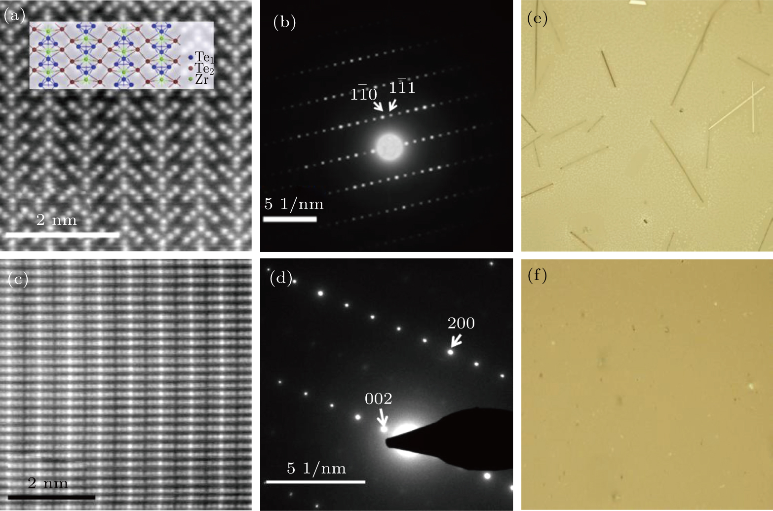
(a)–(d) Aberration corrected TEM images of ZrTe5 nanoribbon. The nanoribbon is about 50 nm thick. (a) HAADF image. Inset, atomic structure model of ZrTe5 in the (110) plane. (c) HAADF image in the (010) plane. (b), (d) Electron diffraction pattern along the [110] and [010] directions. (e) Optical micrograph of a mica substrate after growth in presence of a silicon substrate. ZrTe5 ribbons can be found. (f) Optical micrograph of a mica substrate after growth without a silicon substrate. No ZrTe5 can be found.
