† Corresponding author. E-mail:
Project supported by the National Key R&D Program of China (Grant No. 2016YFF0200402).
Large-scale Josephson junction (JJ) arrays are essential in many applications, especially quantum voltage standards application for which hundreds of thousands of junctions are required to realize a high quantum voltage. For almost all applications, high-quality JJ arrays must be realized in a small chip area. This study proposes vertically quadruple-stacked Nb/(NbxSi1 – x/Nb)4 JJs to increase the integration density of junctions in an array. The current–voltage (I–V) characteristics of a single stack of Nb/(NbxSi1 – x/Nb)4 JJs have been measured at 4.2 K. The uniformity of junctions in one stack and the uniformity of several stacks over the entire 2 inches wafer have been analyzed. By optimizing the fabrication parameters, a large-scale quadruple-stacked Nb/(NbxSi1 – x/Nb)4 array consisting of 400000 junctions is realized. Good DC I–V characteristics are obtained, indicating the good uniformity of the large-scale array.
If a Josephson junction (JJ) is driven at frequency f, then its current–voltage (I–V) curve will develop constant voltage regions at nh f/2e, where n is an integer; e is the elementary charge; and h is the Planck constant. With a typical applied microwave frequency of 18 GHz, one junction can only output a quantum voltage of ∼ 37 μV for the first step. Therefore, hundreds of thousands of JJs must be connected in series to output a high quantum voltage. Large-scale JJ arrays are essential in many applications, especially for quantum voltage standards applications.[1–4] For example, ∼ 0.3 million JJs are required for a quantum voltage of 10 V.[5–7] High-quality large-scale JJ arrays are clearly crucial for quantum voltage chip applications. Superconductor–normal metal–superconductor (SNS) JJs are usually used in the voltage standards.[4]
To increase the number of JJs in an array, they are often stacked vertically. This arrangement not only saves space in a chip but also reduces the branches of the coplanar waveguide (CPW). For programmable voltage standards, this can increase the output voltages for a given microwave drive frequency and chip area; for the ac voltage standard, it can increase the output voltage, output bandwidth, and operating margins. Therefore, to optimize the performance of the voltage standards, studies have tried to pack junctions more densely. The National Institute of Standards and Technology (NIST), USA, uses triple-stacked JJs,[5] whereas Physikalisch-Technische Bundesanstalt, Germany,[6] and National Institute of Advanced Industrial Science and Technology, Japan,[7] use double-stacked JJs. Currently, the National Institute of Metrology, China, has achieved a quantum voltage output of 0.5 V by using triple-stacked JJs.[8] In the present study, we propose large-scale quadruple-stacked SNS JJs to verify the fabrication ability for obtaining large quantum voltages. This junction is designed with the structure Nb/(NbxSi1 – x/Nb)4, where Nb is the superconducting layer and NbxSi1 – x is the normal metal layer. In this design, four JJs are stacked vertically. When 100000 junctions are stacked in a plane, the total number of junctions will be quadrupled. Through improvements in fabrication processes, quadruple-stacked JJs have been fabricated. Large-scale JJ arrays consisting of 100000 stacks or 400000 junctions have been designed and realized. Although NIST has fabricated stacks up to 10 junctions tall of MoSi2 barrier junctions, there are only 1000 stacks in an array.[9] In this study, tall stacks of NbxSi1 – x barrier JJs are realized; furthermore, the integration density is increased compared with that achieved by NIST. The DC I–V curves of these devices are measured and analyzed to test the junction uniformity.
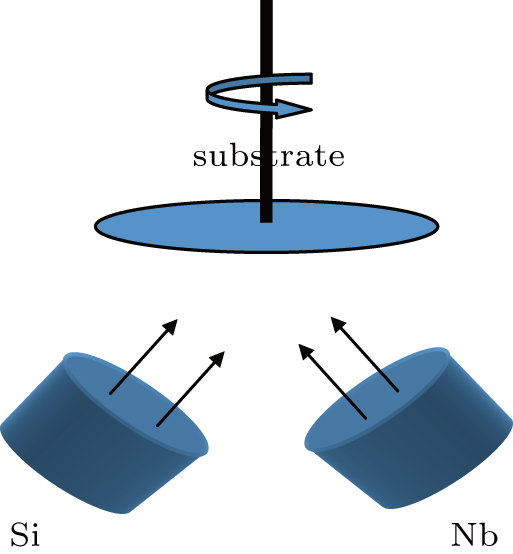
Nb/(NbxSi1 – x/Nb)4 layers are sputtered in situ in a high-vacuum chamber. The sputtering power for the superconducting Nb film is 500 W, and the deposition rate is ∼ 0.75 nm/s. The NbxSi1 – x film is co-sputtered with sputtering powers of 33 W or 36 W for Nb and 248 W for Si, respectively, as shown in Fig.
The main challenge is to fabricate a vertical profile for the junction definition etch of all stacked junctions so that the stacked junctions can have nearly the same junction area and, in turn, the same critical current. A reactive ion etching (RIE) compound with inductively coupled plasma is used to etch the top Nb layer, the alternating Nb middle layer, and the NbxSi1 – x barrier layer. The junction area definition process is optimized compared with previously reported processes.[9,10] Apart from SF6 and C4F8, CHF3 is added to the etching mixture gas. SF6 and CHF3 act as etching gases, whereas C4F8 acts as a passivating gas to protect the junction profile and keep the side facade steep and clean so that the junctions in the stack can remain uniform.
SiO2 is deposited in a plasma-enhanced chemical vapor deposition system and used as an insulating layer. The Nb base electrode is etched using SF6. By contrast, SiO2 is etched using CHF3 and O2. Before depositing the 500-nm-thick Nb wiring electrode, the contact area is subjected to DC-biased RF cleaning. The wire layer is etched by RIE with SF6 again. Figure
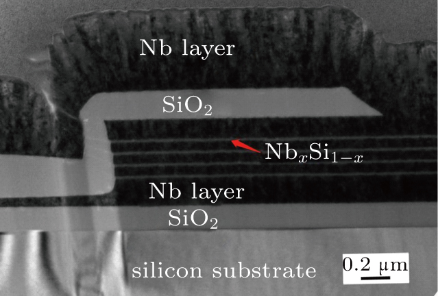
The quality of the etch process is directly observed by transmission electron microscopy (TEM), as shown in Fig.
There are three samples which have been measured at 4.2 K. Table
| Table 1. Characteristics of the quadruple-stacked samples. . |
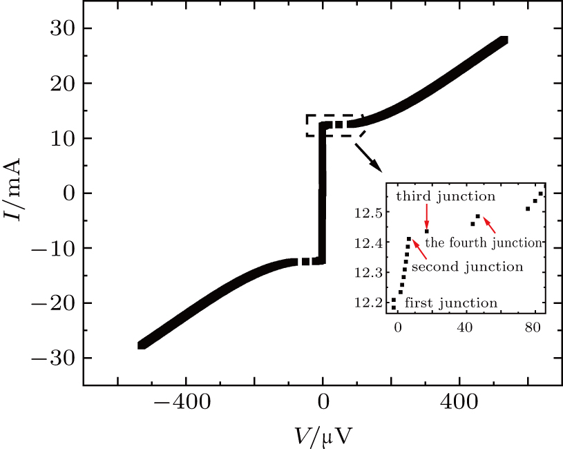
Figure
| Table 2. Critical current spread over in sample No. 1. . |
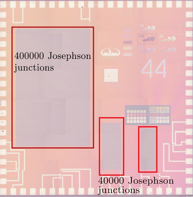
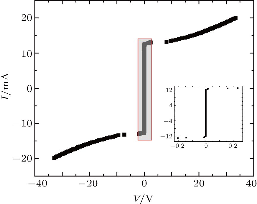
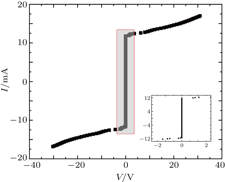
The I–V curves for 40000 and 400000 junctions arrays are also measured at 4.2 K, as shown in Figs.
Single stacks and large-scale arrays of stacks of Nb/(NbxSi1 – x/Nb)4 JJs have been fabricated and measured. The junctions in one stack over the 2 inches substrates exhibit a uniform critical current. This result shows that JJ arrays can be designed and fabricated to output a higher quantum voltage. Further, the I–V curve of the junctions arrays containing 100000 stacks or 400000 junctions also exhibits a uniform shape and critical current. This study represents a breakthrough in the efforts toward realizing a higher voltage standard at NIM.
| [1] | |
| [2] | |
| [3] | |
| [4] | |
| [5] | |
| [6] | |
| [7] | |
| [8] | |
| [9] | |
| [10] |


