Scalable preparation of water-soluble ink of few-layered WSe2 nanosheets for large-area electronics
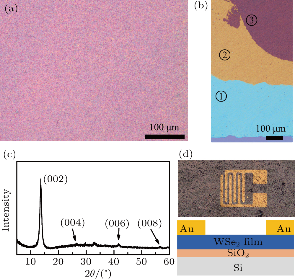
(a) Optical image of a smooth thin film of WSe2 nanosheets. (b) Optical image of layer-by-layer self-assembly thin film of WSe2 nanosheets. Numbers 1–3 indicate the layers of WSe2 films, the regions with different colors show the films with different thicknesses. (c) XRD pattern of the resulting thin film displaying only {001} planes. (d) Schematic configuration and optical images of the back-gate WSe2 thin-film transistors on the 300-nm-thick SiO2/Si substrate.