Scalable preparation of water-soluble ink of few-layered WSe2 nanosheets for large-area electronics
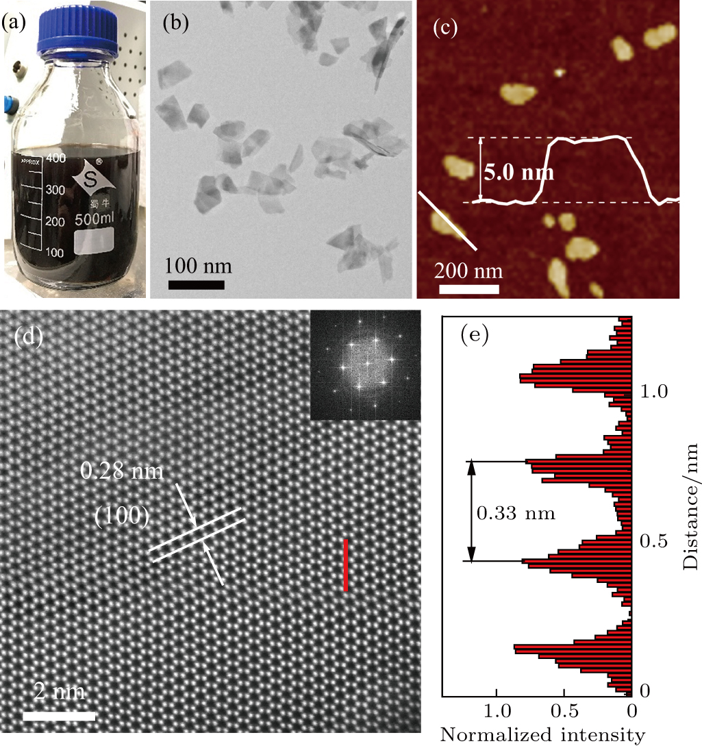
(a) Photograph of exfoliated WSe2 nanosheets dispersed in aqueous NaDC solution. (b) TEM and (c) AFM images of WSe2 nanosheets, the inset pattern in (c) is the cross-sectional height profile. (d) HAADF STEM image of WSe2 nanosheets, the FFT pattern is shown in the inset. (e) The signal intensity of atoms along the red line in (d) showing the same contrast value, corresponding to the lattice constant of 0.33 nm.
