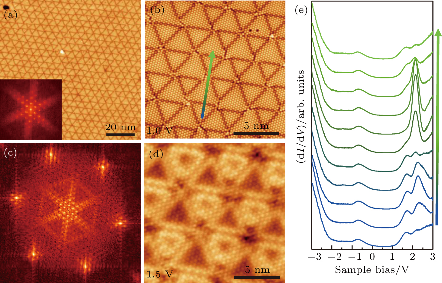
Formation of Se-
3
monolayer on Au(111) at 250 °C. [(a), (b), (d)] Large-scale and atomic-resolution [(b), (d)] STM images of Se-
3
monolayer. The inset in panel (a) is the corresponding FFT image. (c) FFT image of the atomic-resolution STM image of Se-
3
monolayer with a scanning area of 25 nm × 25 nm. (e) Series of d I/d V spectra taken along the line indicated in panel (b). Tunneling conditions: (a) Vbias = –2.0 V, Iset = 200 pA; (b) Vbias = 1.0 V, Iset = 500 PA; (d) Vbias = 1.5 V, Iset = 500 pA; (e) Vbias = –2.0 V, Iset = 500 pA. |