† Corresponding author. E-mail:
Project supported by the National Natural Science Foundation of China (Grant No. 51673214) and the National Key Research and Development Program of China (Grant No. 2017YFA0206600).
The morphology and interface of perovskite film are very important for the performance of perovskite solar cells (PSCs). The quality of perovskite film, fabricated via two-step spin-coating process, is significantly influenced by the morphology and crystallinity of PbI2 film. With the addition of additive dimethyl sulfoxide (DMSO) into the PbI2 precursor, the roughness and trap-state density of perovskite film have been significantly reduced, leading to the excellent contact between perovskite layer and subsequent deposited carrier transport layer. Accordingly, the planar heterojunction PSCs with an architecture of ITO/SnO2/perovskite/PTAA/Ag show an efficiency up to 19.02%. Furthermore, PSCs exhibit promising stability in air with a humidity of ∼ 45%, and retain 80% of initial efficiency after being exposed to air for 400 h without any encapsulation.
Perovskite solar cells (PSCs) have attracted much attention due to their spectacular breakthroughs in the past ten years, ascribed to the brilliant photovoltaic properties of perovskite materials[1–4] and modification of alternative functional layers.[5,6] Up to now, the certified power conversion efficiency (PCE) has been enhanced to 25.2%,[7] reflecting the promising commercial applications of PSCs. The PCE of PSCs relies on efficient charge carrier extraction at interfaces.[8] The quality of perovskite layer and the properties of charge transport layers, i.e., hole transport layer (HTL) and electron transport layer (ETL), are the two key factors that affect the interfacial contact, especially the HTL in PSCs with n–i–p configuration. Poly[bis(4-phenyl)(2,4,6-trimethylphenyl)amine] (PTAA) is a stable p-type polymer with high hole mobility and suitable energy level. Thus, it has been used as the HTL in PSCs since the early stage in the development of PSCs because of its prominent transport ability.[9] In fact, considerably high PCE of 22.1% was achieved for PSCs with PTAA as the HTL.[10] However, the interfacial contact between perovskite and PTAA is a thorny problem in n–i–p structural PSCs due to the hydrophobic property of PTAA.
A lot of strategies have been suggested to improve the interfacial contact between the perovskite and PTAA. Solvent engineering assisted one-step solution deposition was introduced to achieve PTAA-based PSCs with a PCE of 16.2%.[11] The high fill factor (FF) over 75% was achieved in this device, which is ascribed to the exquisite interface contact between MAPbI3 and PTAA derived from the modification of perovskite grain and surface. Meanwhile, PTAA-based graded heterojunction was achieved for good interface between perovskite and HTL by involving PTAA in the anti-solvent, one-step solution deposited perovskite.[12]
Two-step sequential deposition has been widely used to fabricate perovskite film and accordingly produce efficient PSCs.[13–17] Nevertheless, because of the complexion of reaction, it is still difficult to control the nucleation and growth of perovskite crystal. Thus, the perovskite film often shows incomplete conversion and poor surface roughness,[18,19] which are disadvantageous to the stability and the interfacial contact between perovskite and other functional layers. It was reported that the large molecular mass of PTAA induces a rough contact between PTAA and perovskite, leading the performance of PSC with n–i–p architecture to degenerate.[20] Several methods have been proposed to modify the perovskite films via two-step sequential process by controlling PbI2 film through manipulating the PbI2 precursor, including adding water,[21] PCBM,[22] 1,8-diiodooctane (DOI),[23] hydroiodic acid (HI),[24] hydrochloric acid (HCl),[25] etc.
Here in this work, PTAA as the HTL is introduced to fabricate planar heterojunction (PHJ) PSCs with n–i–p architecture. The active layer perovskite composed of triple cations 

The materials were purchased without further purification, including: NH2CH = NH2I (FAI) (99.5%, Xi’an Polymer Light Technology Corp.), CH3NH2Br (MABr) (99.5%, Xi’an Polymer Light Technology Corp.), CH3NH2Cl (MACl) (99.5%, Xi’an Polymer Light Technology Corp.), CsI (99%, Strem Chemicals, Inc.), PbI2 (99%, Tianjing Weiyi Chemical Technology Co., Ltd), SnO2 (15% in H2O colloidal dispersion,Alfa Aesar), PTAA (Mw = 33500 g/mol, Xi’an Polymer Light Technology Corp.), Spiro-OMeTAD (99%, Wuhan Zhuojia Technology Co., Ltd), isopropanol (IPA) (99.5%, J & K Scientific), DMF (99.8%, Sigma-Aldrich), DMSO (99.8%, Sigma-Aldrich), chlorobenzene (CB) (99.8%, Sigma-Aldrich), and acetonitrile (99.95%, Sigma-Aldrich).
The patterned ITO was washed by acetone, deionized water, deionized water with detergent, IPA in an ultrasonic cleaner for 20 min, in sequence, followed by UV-ozone treatment for 25 min. The SnO2 colloidal dispersion (with diluted concentration of 2.67%) was spin-coated onto ITO/glass substrate at 3000 rpm for 30 s. Then the film was annealed at 150 °C for 30 min. In the process of two-step sequential deposition of perovskite film, PbI2 precursor solutions were prepared by dissolving 599.3 mg PbI2 and 35 mg CsI in 1 mL DMF and DMSO mixed solvent with 4 types of volume mixing ratios (DMF : DMSO = 10 : 0, 9.5 : 0.5, 9 : 1, 8 : 2, which were named DMSO-0%, DMSO-5%, DMSO-10%, DMSO-20%, respectively) and were stirred at 75 °C overnight. The PbI2 film was obtained by spin-coating PbI2 precursor onto SnO2-coated substrate at 1500 rpm for 30 s, followed by being annealed at 70 °C for 30 min. Then, FAI:MABr:MACl mixed solution (60 mg:6 mg:6 mg in 1 mL IPA) was spin-coated at 1500 rpm for 30 s. The perovskite film could be formed by heating the as-prepared film at 150 °C for 20 min under ambient conditions with a relative humidity of about 40%. The HTL was deposited by spin-coating PTAA solution with 12.5 mg PTAA dissolving in 1 mL toluene with an additive of 9.4 μL Li-TFSI solution (170 mg Li-TFSI in 1 mL acetonitrile) and 5 μL TBP at 3000 rpm for 30 s. For the Spiro-OMeTAD HTL, Spiro-OMeTAD solution prepared by dissolving 90 mg Spiro-OMeTAD, 45 μL Li-TFSI solution (170 mg Li-TFSI in 1 mL acetonitrile), and 10 μL TBP in 1 mL chlorobenzene, was deposited with the same spin-coating parameter as the PTAA HTL. Finally, the Ag electrode was deposited by thermal evaporation with a fixed area of 0.09 cm2 through using metal mask. For evaluating the trap densities of perovskite, electron-only devices were created. The PCBM solution could be obtained by dissolving 20 mg PCBM into 1 mL chlorobenzene and stirring at 75 °C overnight. The spin-coating parameter of PCBM ETL was fixed at 3000 rpm for 30 s, without annealing process after being spin-coated.
The absorbance spectra and crystallographic properties of PbI2 and perovskite films were obtained by ultraviolet-visible spectrophotometer (UV-vis, Puxi, T9, China), x-ray diffractometer (XRD, Rigaku D, Max 2500, Japan), respectively. The morphology of PbI2 and perovskite films were revealed by scanning electron microscope (SEM, FEI Helios Nanolab 600i SEM, America) and atomic force microscope (AFM, Agilent Technologies 5500AFM/SPM System), respectively, and the element composition of PbI2 film was measured by the energy dispersive spectrometer (EDS). A digital source meter (Keithley, model 2420) was employed to measure the photovoltaic performance of as-prepared PSCs, with a scanning range from +1.2 V to −0.2 V, a 50-ms scanning delay, and 100 points in both reverse- and forward-scan modes, under a xenon-lamp-based solar simulator (Newport 91160 s, AM 1.5 G), whose light intensity of 100 mW/cm2 had been calibrated by a standard silicon solar cell. To obtain the I–V curves of electron-only devices, the corresponding devices were measured under dark condition by a digital source meter, with increasing voltage from 0 V to 1.5 V applied and varied current recorded. The stability measurement was carried out under the J–V measurement condition and the statistics under forward-scan mode were recorded, after that the devices were stored under dark condition with a humidity of ∼ 40%.
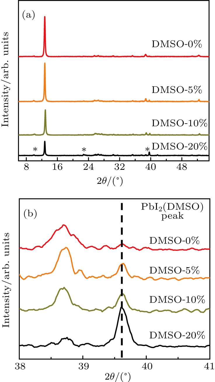
The PbI2 precursors are made with the different solvents, i.e., DMF : DMSO = 10 : 0, 9.5 : 0.5, 9 : 1, 8 : 2, which are named DMSO-0%, DMSO-5%, DMSO-10%, DMSO-20%, respectively. In order to disclose how the additive DMSO influences the crystallization of PbI2 film, the XRD experimental results of PbI2 films are shown in Fig.
 | Fig. 1. (a) XRD patterns of PbI2 derived from different solvents. Star marked peaks are ascribed to PbI2 (DMSO) complex phase. (b) Magnified XRD patterns in region of 2θ from 38° to 41°. |
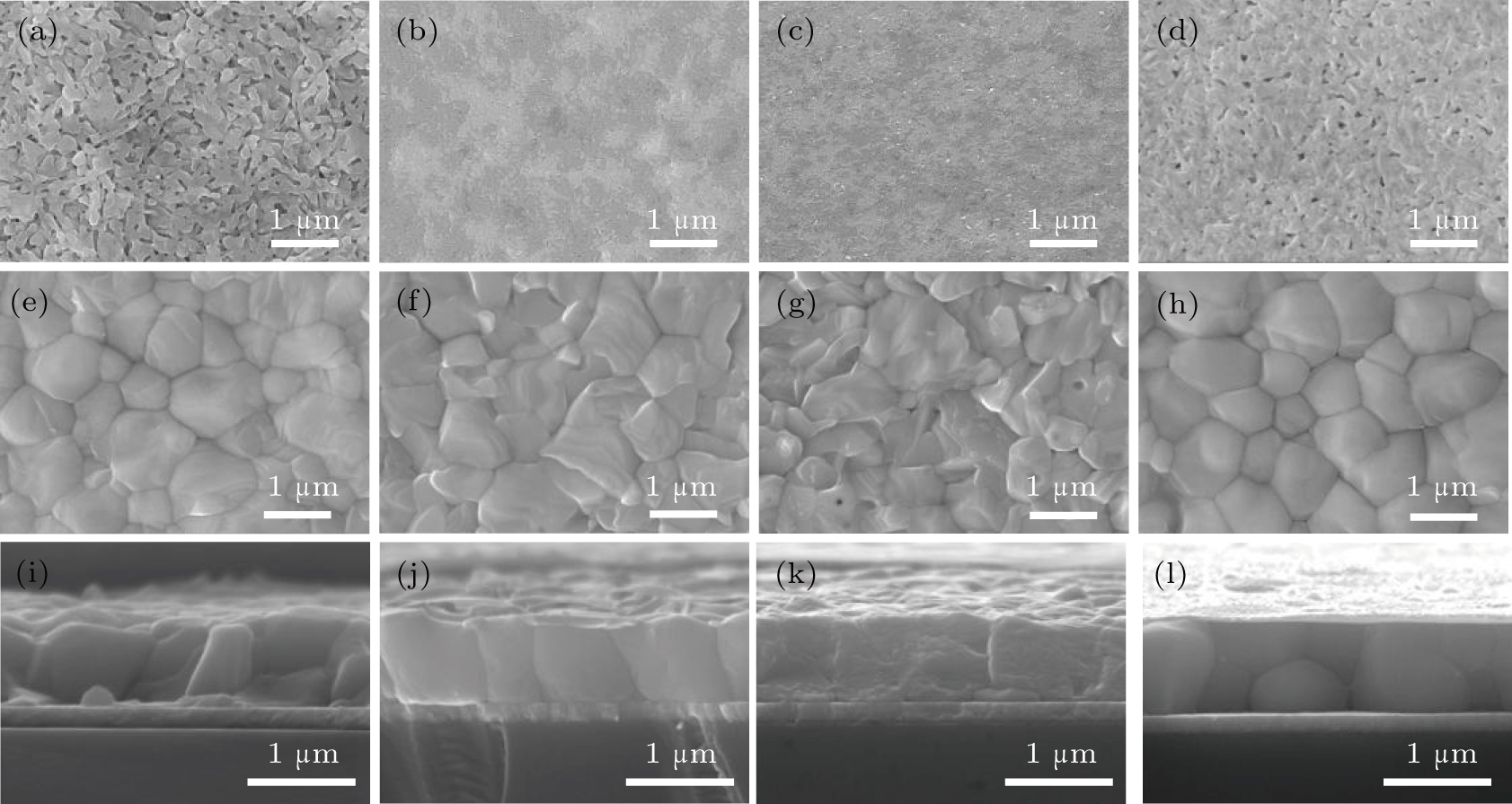
The morphologies of PbI2 films derived from the different solvents are revealed by SEM as illustrated in Figs.
The thermo-gravimetric analysis indicates that the PbI2(DMSO) complex starts to decompose around 100 °C.[27] The PbI2(DMSO) film post-annealed at 70 °C for 30 min contains little trace of PbI2(DMSO) composite with the majority of DMSO molecules escaping from the system. The judgement can be also verified by no obvious shallow color corresponding to FAI-DMSO-PbI2 intermediate phase appearing in the second step of two-step deposition. The post-annealing treatment is speculated to account for this phenomenon, and the PbI2-DMSO composite just exists in an intermediate. Therefore, the DMSO mainly affects the growth and morphology evolution of PbI2 film. The little trace of PbI2(DMSO) complex in the as-prepared PbI2 film has light influence on the subsequent reaction.
The morphology evolution of PbI2 film can be explained by the conversion of PbI2(DMSO) complex in DMF solvent to PbI2(DMSO) intermediate in wet film, and finally to the as-prepared precursor film after DMSO molecule escaping. In the case of DMSO-0%, the PbI2 coordinates with DMF, forming one-dimensional structure along the a axis.[28] During PbI2 film annealing, the DMF volatilizes from the wet film quickly and dendrite-like crystals tend to appear along the a axis. When the DMSO is incorporated, micella-shaped PbI2(DMSO) complex forms with a certain concentration dispersed into DMF uniformly. It has been verified that the DMSO can inhibit the crystallization of PbI2 when PbI2 coordinates with DMSO molecule.[29] Therefore, the final precursor films derived from DMSO-5% and DMSO-10% show sphere-shaped grains with dense, flat morphology. With the DMSO increasing to 20%, the PbI2(DMSO) complex is accumulated and the intermediate tend to be PbI2(DMSO)2,[26] which causes the macroscopic needle-like microcrystal to appear in solvent. After being annealed, the flake-like PbI2 grains originating from the needle-like intermediate appears with DMSO molecule escaping and the remaining DMSO is coordinated with PbI2 to form the PbI2(DMSO) complex, which has been proved by the XRD analysis.
High-quality PbI2 layer can play an important role in the subsequently depositing the perovskite layer in two-step spin-coating process. Figures
The perovskite films are characterized by XRD and shown in Fig.
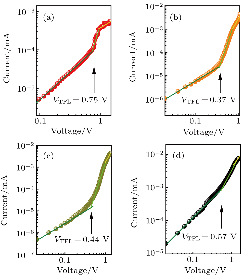
For determining the trap densities of perovskite films, the dark I–V curves of electron-only devices are measured with configuration of ITO/SnO2/perovskite/PCBM/Ag (Fig.

 | Fig. 4. Dark I–V curves of electron-only devices for perovskite films derived from (a) DMSO-0%, (b) DMSO-5%, (c) DMSO-10%, and (d) DMSO-20%, respectively. |
Not only does the quality of perovskite film play a crucial role in the operation of PSCs, but also the interfacial contact does. For investigating the contact between the perovskite layer and the PTAA layer, the AFM is employed to measure the roughness of perovskite films and the results are shown in Fig.
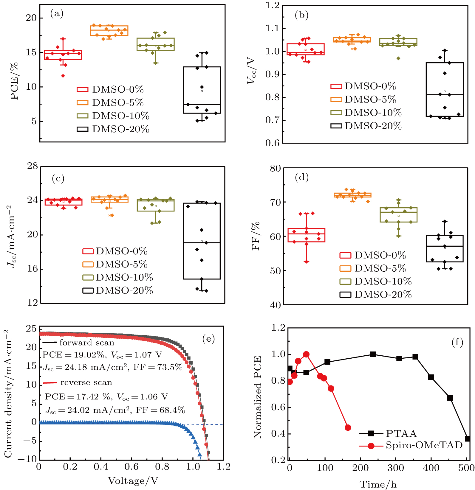
The photovoltaic performance parameters of PSCs are shown in Fig.
However, in the cases of DMSO-0% and DMSO-20% devices, the PCEs of devices diminish greatly and spread in a large range because of the decrease in Voc, Jsc, and FF, as well as the bad stability. The loose contact of grains with many gaps and rough surface result in poor contact between perovskite layer and HTL, and induce the charge carriers to severely combine with each other or the current to leak during the operation of PSCs, which results in the performance deterioration. On the contrary, because of the lower trap density, smooth perovskite film, and exquisite interface contact between perovskite and PTAA, the PSC prepared from DMSO-5% shows the best efficiency, with a typical forward scanning PCE of 19.02% and an average FF of over 70% under 1-sun illumination, Additionally, as shown in Fig.
| Table 1. Average photovoltaic performance parameters of PSCs derived from DMSO-0%, DMSO-5%, DMSO-10%, and DMSO-20%, respectively. Statistical data are based on 12 devices. The highest PCEs are shown in brackets. . |
By optimizing the ratio of DMSO to DMF in PbI2 precursor, the morphology of PbI2 film becomes controllable, which significantly affects the nucleation, growth and ripening process. A suitable crystallinity and morphology of PbI2 film have a significant influence on the quality of subsequent perovskite film prepared by the two-step deposition. The dense, smooth and low-trap density perovskite films could be prepared by preparing high-quality PbI2 substrate, which gives rise to the exquisite interface contact between perovskite and PTAA. The exquisite interface promotes the separation and transport of charge carriers, and thus boosting the PCE up 19.02%. A simple and facile modified two-step sequential deposition technique is developed by precisely adjusting the content of DMSO, which is believed to be helpful for the large-area fabrication of PSC.
| [1] | |
| [2] | |
| [3] | |
| [4] | |
| [5] | |
| [6] | |
| [7] | |
| [8] | |
| [9] | |
| [10] | |
| [11] | |
| [12] | |
| [13] | |
| [14] | |
| [15] | |
| [16] | |
| [17] | |
| [18] | |
| [19] | |
| [20] | |
| [21] | |
| [22] | |
| [23] | |
| [24] | |
| [25] | |
| [26] | |
| [27] | |
| [28] | |
| [29] | |
| [30] | |
| [31] | |
| [32] | |
| [33] | |
| [34] |


