Stackable luminescent device integrating blue light emitting diode with red organic light emitting diode
Su Kang1, 2, Li Jing1, 2, †, Ge Chang1, 2, Lu Xing-Dong1, 2, Li Zhi-Cong1, 2, Wang Guo-Hong1, 2, Li Jin-Min1, 2
Research and Development Center for Semiconductor Lighting, Institute of Semiconductors, Chinese Academy of Sciences, Beijing 100083, China
Center of Materials Science and Optoelectronics Engineering, University of Chinese Academy of Sciences, Beijing 100049, China


† Corresponding author. E-mail: lijing2006@semi.ac.cn

Project supported by the National Key Research and Development Program of China (Grant No. 2017YFB0404800).

Abstract

We present a novel stackable luminescent device integrating a blue light emitting diode (LED) with a red organic LED (OLED) in series. The anode of the OLED is connected with the cathode of the LED through a via in the insulation layer on the LED. The LED–OLED hybrid device is electroluminescent and two electroluminescence (EL) peaks (the blue peak around 454 nm and the red peak around 610 nm) are observed clearly. The effect of the indium tin oxide (ITO) layer on the device performance is analyzed. Compared with the individual LED and OLED, their combination shows great potential applications in the field of white lighting, plant lighting, and display.

1. Introduction

Recently, light emitting diodes (LEDs),[13] organic LEDs (OLEDs),[410] polymer LEDs,[1115] and other solid-state lighting devices have received increasingly attention in the field of lighting. Meanwhile, the blue LEDs + yellow phosphor (YAG:Ce) has become the mainstream because of its high luminous efficiency, low energy consumption, and long lifetime. At present, the commercial white LEDs (WLEDs) based on blue LEDs and YAG:Ce have a luminous efficiency of up to 150 lm/W. However, due to the absence of red light in the spectrum, the low color rendering index (CRI) (Ra < 80) and high correlated color temperature (CCT > 4500 K) are hardly remedied for the commercial WLEDs.[1619] Accordingly, the WLEDs combining red, green, and blue (RGB) LEDs were introduced to improve the CRI and reduce the CCT. Nevertheless, the combination of RGB LEDs had low efficiency, complex manufacturing process, and high cost. In the plant factory, the similar combination of blue and red LEDs was utilized to meet the blue light ranging from 400 nm to 510 nm and the red light ranging from 610 nm to 720 nm demanded for the plant growth.[20]

In the field of LED display, the Mini-LED 4 K/8 K displays with dot pitch less than 0.5 mm will be widely used in the conferences and command centers while the Micro-LED displays with dot pitch less than 50 μm have received widespread attention due to the applications in augmented reality (AR) and virtual reality (VR). Because it is impossible to grow GaN materials for green and blue LEDs and GaAs materials for red LEDs on the same wafer, the full-color LED displays are manufactured by arranging the blue, green, and red discrete LEDs on the printed circuit board (PCB) by the chip on board (COB) process.[21] However, this scheme severely restricts the further reduction of the pixel pitch and affects the enhancement in resolution. In addition, the micro flip-chip red LEDs have a complicated manufacturing process, low yield, and high cost due to the removal of the conductive and opaque GaAs substrate. It is also a challenge for micro red LEDs based on GaAs to reach a higher external quantum efficiency (EQE).

In order to solve the application problems of LEDs mentioned above, we try to introduce the OLEDs into the field of LED lighting and display. On the one hand, it can be more easily realized for lighting with high CRI to stack the red OLED on the green and blue LEDs. On the other hand, the display with ultra-small pixel pitch can be accomplished by arraying the green and blue LEDs and red OLEDs. The EQE of the red phosphorescent OLEDs can achieve 35.6%,[22] which makes it possible to combine blue and green LEDs with red OLEDs.

In this paper, we explore the process compatibility between LEDs and OLEDs and prepare a stackable luminescent device combining a blue LED with a red OLED. The photoelectric parameters are measured and analyzed. The approach to combining LEDs with OLEDs is extremely novel and this work lays a foundation for the subsequent research on white lighting devices and full-color displays that combine LED and OLED.

2. Experiment

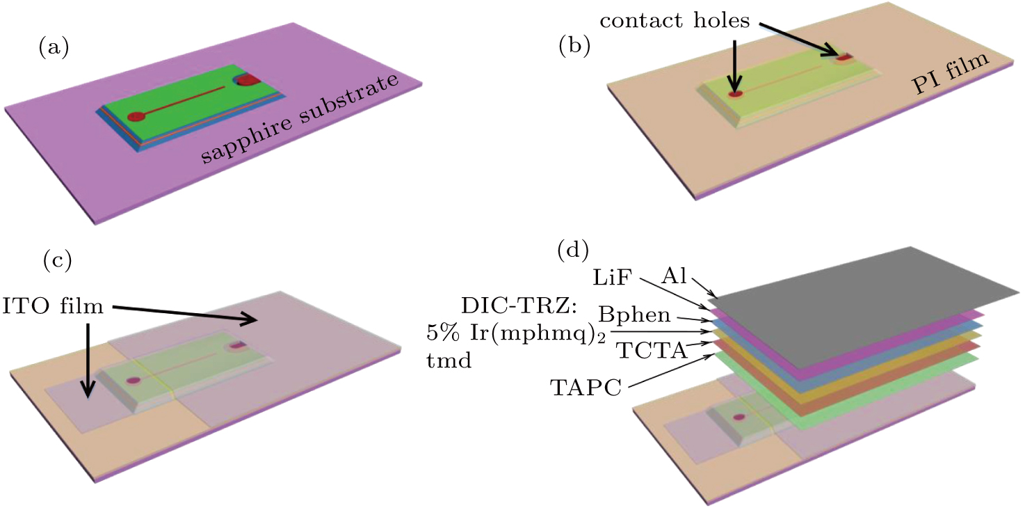
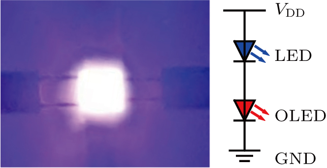
The stackable luminescent device was obtained through the fabrication of InGaN/GaN-based blue LEDs and the process of conventional red OLEDs. Firstly, the epitaxial structure of blue LEDs was grown on a 2″ c-plane patterned sapphire substrate (PSS) by the metal–organic chemical vapor deposition (MOCVD), which was composed of a 4.0-μm-thick undoped GaN buffer layer, a 2.0-μm-thick Si-doped n-GaN layer, 9 pairs of InGaN (2.4 nm)/GaN (14 nm) multiple quantum wells (MQWs), a 40-nm-thick p-AlGaN electron blocking layer, and a 100-nm-thick Mg-doped p-GaN layer. Then, a 280-nm-thick indium tin oxide (ITO) layer was deposited by the electron beam (EB) evaporation technique onto the wafer as the current spreading layer as well as the ohmic contact layer of p-type GaN. Next, the mesa structure was successively formed by the photolithography and inductively coupled plasma-reactive ion etching (ICP-RIE) process. Subsequently, Cr/Al/Cr/Pt/Au metal layers were deposited by electron-beam evaporation and patterned by a lift-off process. The structure of the LED device was almost formed as shown in Fig. 1(a). Afterwards, a photosensitive polyimide film was deposited by the spin-coating method and the contact holes were formed by the exposure and development technique as shown in Fig. 1(b). And the polyimide film was cured into an insulating layer by baking. Then, an ITO layer was deposited by the EB evaporation technique. After the ITO layer was patterned by the photolithography process, the extraction electrode contacted with p-pad of the LED and the anode of the OLED contacted with n-pad of the LED were formed as shown in Fig. 1(c). Finally, the rest of the red OLED was formed with the vacuum thermal evaporation technique. A conventional structure of ITO/TAPC (30 nm)/TCTA (10 nm)/DIC-TRZ: 5% Ir(mphmq)2tmd (30 nm)/Bphen (30 nm)/LiF (1 nm)/Al (150 nm) was introduced into the red OLED as shown in Fig. 1(d). The stackable luminescent device was bottom-emitting and consisted of a blue LED connected in series with the red OLED. The equivalent circuit diagram of the integrated LED–OLED device and the direct view image are shown in Fig. 2. Due to the lack of relevant equipment, this device is not packaged to isolate water vapor and oxygen. However, all the parameters in this study were measured for the first time.

Fig. 1. Fabrication steps of stackable luminescent device: (a) structure of LED device after depositing ITO on p-GaN, ICP etching for forming mesa structure and depositing multilayer metal films, (b) spin coating of photosensitive PI film and forming contact holes, (c) depositing ITO on cured PI film, (d) depositing the rest of red OLED.
Fig. 2. Direct view image (left) and equivalent circuit diagram of integrated LED–OLED device (right).
3. Results and discussion

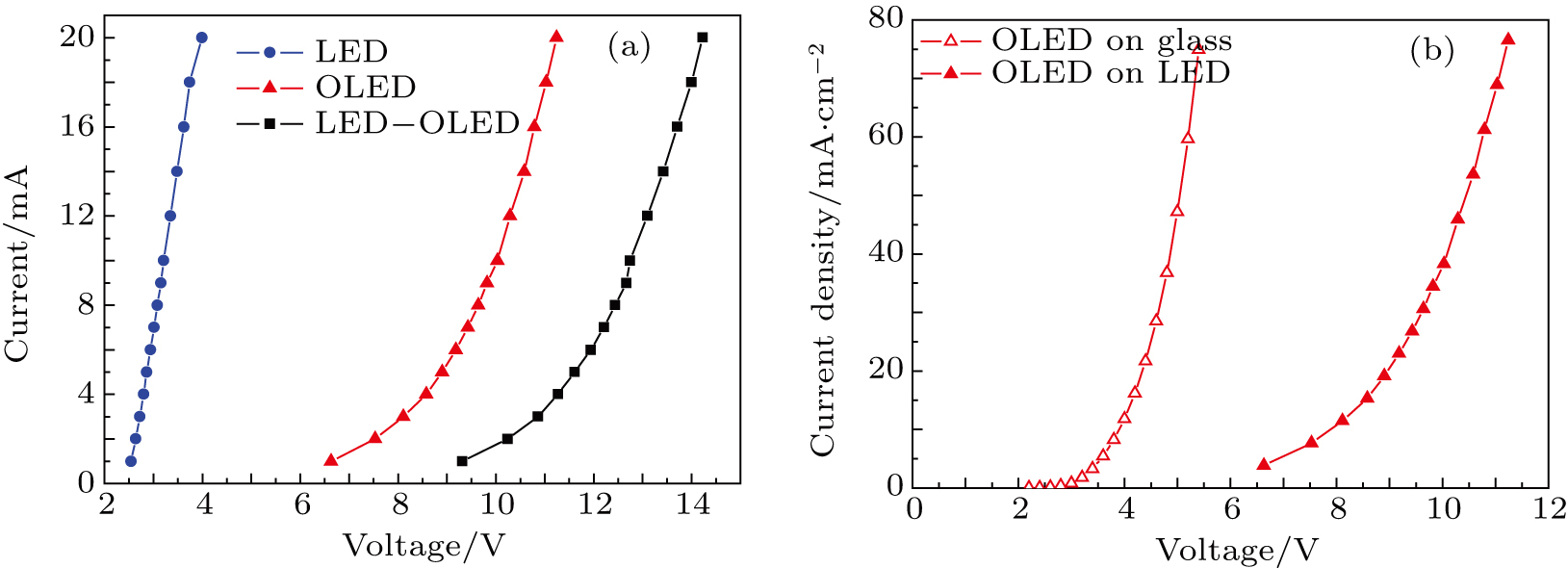
Figure 3(a) shows the IV characteristics of the blue LED, red OLED, and LED–OLED hybrid optical device. When the forward current is 5 mA, the voltages of the LED, OLED, and the hybrid optical device are 2.86 V, 8.9 V, and 11.61 V, respectively. The voltage of the LED is normal while that of the OLED is a little higher. The JV curve of the OLEDs on the LED and on the ITO-coated glass are compared in Fig. 3(b). The voltage of the OLED on the LED is higher at the same current density, especially at the high current density, which is caused by the material quality and surface flatness of the ITO. The ITO is deposited on the glass by the magnetron sputtering and the commercial ITO-coated glass is flatted by being polished. However, the ITO is deposited on the LED by the electron beam evaporation technique as mentioned above. And the ITO layer is not subjected to recrystallization any more, because the multilayer metal films of the LED cannot withstand such high temperatures of rapid thermal annealing (RTA). This resulted in a higher resistivity of the ITO layer. The effect of RTA on resistance of ITO is further studied. As shown in Table 1, the square resistance (R) of ITO decreases to 76% after RTA according to the four experiments. Therefore, it can be predicted that the voltage of OLED can also drop to 76% approximately. As the current density increases in the measurement range (from 3.83 mA/cm2 to 76.56 mA/cm2), the voltage of the OLED on the LED will decrease accordingly from 1.59 V to 2.70 V. Besides, the roughness of ITO surface is also improved after RTA as reported in Ref. [23]. Hence, the electrical properties of the OLED is sacrificed in order to ensure the performance of the LED. In addition, the surface of the LED is patterned and fluctuant, which affects the roughness of the ITO surface and the performance of the OLED as well. It can be expected that the electrical properties of the OLED will be greatly improved if the multilayer metal films of the LED are replaced with the thermostable metal and dry etching damage is removed by being treated in tetramethylammonium hydroxide (TMAH).[24,25] The voltage of the OLED will significantly decrease after optimizing the quality and flatness of the ITO film by the processes as mentioned above.

Fig. 3. (a) The IV characteristics of blue LED, red OLED, and LED–OLED hybrid optical device, and (b) JV curve of OLEDs on LED and on ITO-coated glass.
Table 1.

Square resistance (R) of 100-nm-thick ITO before and after RTA.

.

The electroluminescence (EL) spectra of the LED–OLED hybrid optical device under various current injections are shown in Fig. 4. It can be clearly seen that two EL peaks (the blue peak around 454 nm and the red peak around 610 nm) are observed and the intensity of blue peak has a large proportion in each spectral curve. As the injection current increases, a blueshift has been found for the blue EL peak position, which is attributed to the quantum confined Stark effect (QCSE) and the band filling effect for the InGaN/GaN LEDs.[26,27] The illustration shows the EL spectrum of the blue LED, red OLED, and LED–OLED hybrid device measured respectively when the injection current is 3 mA. The spectrum of hybrid device is almost the superposition of the spectrum of the blue LED and the spectrum of the red OLED, which demonstrates that the integration does not degrade their performances. This device exhibits two emission bands peaked, respectively, at 454 nm and 610 nm, which corresponds to the wavelength region of plant lighting.
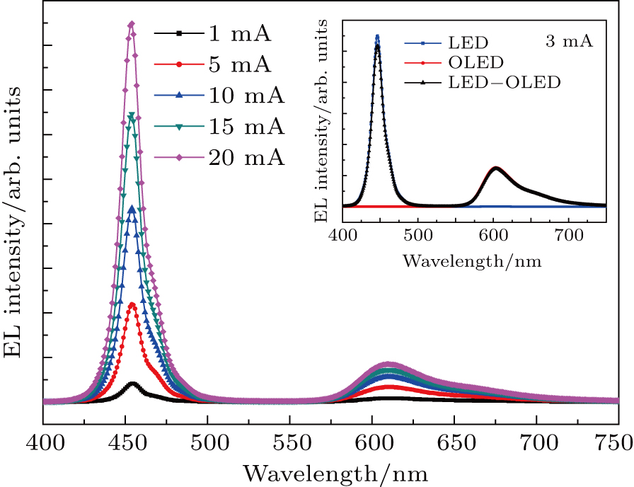
Fig. 4. EL spectra of LED–OLED hybrid optical device under various current injections with inset showing EL spectrum of blue LED, red OLED, and LED–OLED hybrid device at 3 mA.

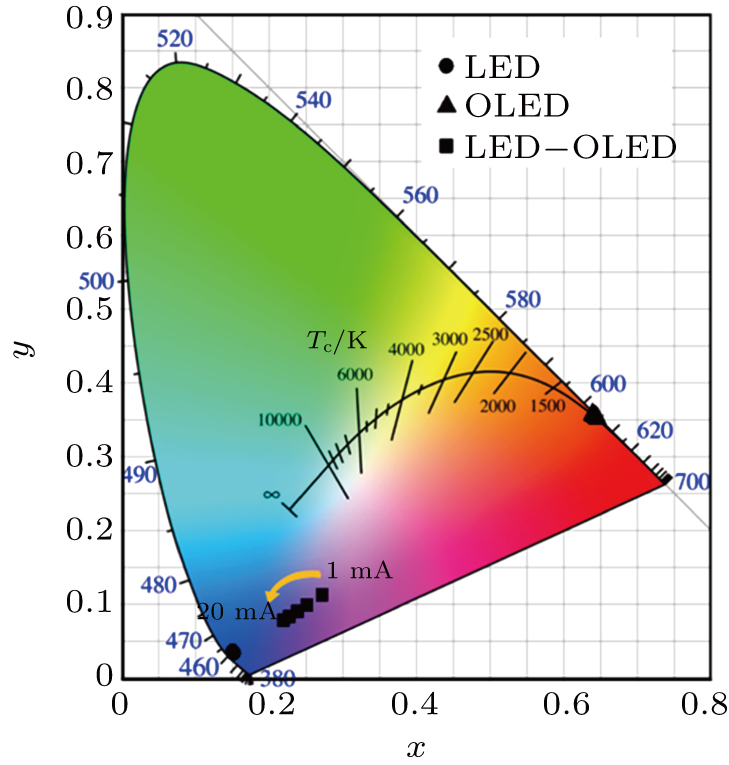
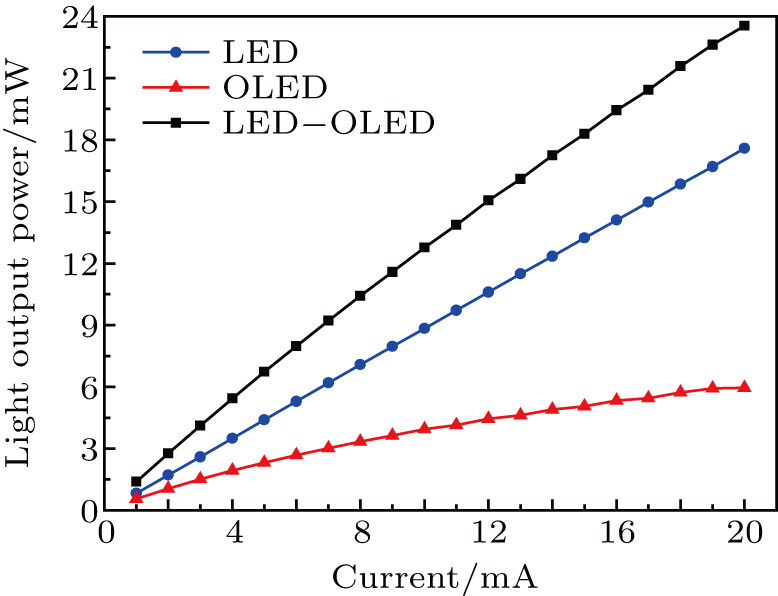
The light output power (LOP) of the LED, OLED, and the hybrid optical device under various current injections are shown in Fig. 5. It can be found that the LOP of the hybrid optical device increases monotonically with the injection current increasing. When the injection current is increased to the 20 mA, the LOP of OLED becomes saturated gradually while the LOP of LED increases linearly approximately. Besides, the LOP of the blue LED is much higher than that of the red OLED. As the current increases, the emitting intensity ratio of the LED to the OLED becomes larger. This is also reflected in the color coordinates of the LED–OLED hybrid optical device in Commission Internationale de L’Eclairage (CIE) 1931 chromaticity diagram as shown in Fig. 6. We assume that the two light sources have the chromaticity coordinates (x1, y1) and (x2, y2). According to the formula of color mixing[28]

where L1 and L2 are the factors positively correlated with the LOP of the two light sources. It can be found that the chromaticity coordinate of the mixed light is a linear combination of the individual chromaticity coordinates weighted by the Li (i = 1, 2) factors. Besides, the chromaticity coordinate of mixed light (x, y) approaches to (x1, y1) if the L1 increases faster than L2. Thus, the chromaticity coordinate of the LED–OLED hybrid optical device is close to that of the blue LED. In addition, when the injection current is increased from 1 mA to 20 mA, the chromaticity coordinates of the hybrid optical device shift toward the blue region while that of the LED or OLED are almost constant. It is attributed to the fact that the LOP of the LED is higher and increases faster than that of the OLED.

Fig. 5. Plot of LOP versus injection current of LED, OLED, and hybrid optical devices.
Fig. 6. Color coordinates of LED, OLED, and LED–OLED hybrid optical devices in CIE 1931 chromaticity diagram.

For the LED lighting, unlike the traditional scheme of blue LEDs + yellow phosphor, a novel approach is proposed to achieve EL of the blue LED and red OLED simultaneously without additional drive. However, the brightness and color of the light emitted from the LED and OLED need to be adjusted. According to the EL spectra of the hybrid device in Fig. 4, the non-blue portion of the spectrum needs to be enhanced, which requires the intensity and widening the emission spectrum of the OLED to be improved. The white light source is expected to be implemented by combining the blue LED and the yellow, orange or red OLED with high brightness and wide spectrum.

This study also provides a new idea for fabricating the full-color flat panel display. At the present stage of the development of LED display, the feature of high resolution is pursued, which means that the size of the subpixel is reduced. However, the external quantum efficiency of red LEDs decreases too fast as the size decreases. Besides, the flip-chip red LEDs used for transfer have a complicated manufacturing process and high cost due to the removal of the conductive and opaque GaAs substrate. For the field of OLED display, although the blue phosphorescent OLED has relatively high power efficiency, the operation lifetime is short and the color is sky-blue. By comparison, the lifetime and color of the blue triplet-triplet fluorescence (TTF) OLED are acceptable but the power efficiency is much low.[2931] At the same time, it is worth noting that the blue LEDs and red OLEDs have excellent performances in their respective display fields. This study demonstrates the feasibility of combining blue LEDs with red OLEDs and shows the possibility to realize the full-color flat panel display.

4. Conclusions

In this work, we fabricated a stackable luminescent device integrating a blue LED with a red OLED in series. The LED–OLED hybrid device is a two-terminal EL device without additional drive. The EL spectrum indicates that the hybrid device has an excellent lights-mixing effect. However, the photoelectric performance of the red OLED needs to be further optimized. This combination of the blue LED and red OLED has the potential applications in the field of white lighting, plant lighting, and full-color flat panel display.

Reference
[1]Nakamura S Senoh M Iwasa N Nagahama S Yamada T Mukai T 1995 Jpn. J. Appl. Phys. 34 1332
[2]Akasaki I Amano H 1997 Semicond. Semimetals 48 357
[3]Li J M Liu Z Liu Z Q Yan J C Wei T B Yi X Y Wang J X 2016 J. Semicond. 37 061001
[4]D’Andrade B W Forrest S R 2004 Adv. Mater. 16 1585
[5]Reineke S Lindner F Schwartz G Seidler N Walzer K Lussem B Leo K 2009 Nature 459 234
[6]Ying L Ho C L Wu H Cao Y Wong W Y 2014 Adv. Mater. 26 2459
[7]Wang Q Ma D 2010 Chem. Soc. Rev. 39 2387
[8]Meyer J Hamwi S Kroger M Kowalsky W Riedl T Kahn A 2012 Adv. Mater. 24 5408
[9]Yang X Zhou G Wong W Y 2014 J. Mater. Chem. 2 1760
[10]Wu X M Hua Y L Wang Z Q Yin S G Zheng J J Deng J C Petty M C 2006 Chin. Phys. Lett. 23 1012
[11]Shan Q Song J Zou Y Li J Xu L Xue J Dong Y Han B Chen J Zeng H 2017 Small 13 1701770
[12]Si J Liu Y He Z Du H Du K Chen D Li J Xu M Tian H He H Di D Lin C Cheng Y Wang J Jin Y 2017 ACS Nano 11 11100
[13]Protesescu L Yakunin S Bodnarchuk M I Krieg F Caputo R Hendon C H Yang R X Walsh A Kovalenko M V 2015 Nano Lett. 15 3692
[14]Wang P Bai X Sun C Zhang X Zhang T Zhang Y 2016 Appl. Phys. Lett. 109 063106
[15]Song J Li J Xu L Li J Zhang F Han B Shan Q Zeng H 2018 Adv. Mater. 30 e1800764
[16]Wang B Lin H Huang F Xu J Chen H Lin Z Wang Y 2016 Chem. Mater. 28 3515
[17]Wang Z Chu I H Zhou F Ong S P 2016 Chem. Mater. 28 4024
[18]Song E Zhou Y Yang X B Liao Z Zhao W Deng T Wang L Ma Y Ye S Zhang Q 2017 ACS Photon. 4 2556
[19]Du Y Shao C Y Dong Y J Yang Q H Hua W 2015 Chin. Phys. 24 117801
[20]Xu S H Wang X L Wu Y M 2000 Eco-agriculture Res. 8 18
[21]Hu M Y Wu Y P 2014 15th International Conference on Electronic Packaging Technology August 12–15 Chengdu, China 97
[22]Kim K H Lee S Moon C K Kim S Y Park Y S Lee J H Woo Lee J Huh J You Y Kim J J 2014 Nat. Commun. 5 4769
[23]Meng Q Z Fang Y Z Ma Y Li W Z Jin L F 2013 Mater. Sci. 03 45
[24]Kim K W Jung S D Kim D S Kang H S Im K S Oh J J Ha J B Shin J K Lee J H 2011 IEEE Electron Dev. Lett. 32 1376
[25]Tang K Huang W Chow T P 2009 J. Electron. Mater. 38 523
[26]Li L Li P Wen Y Wen J Zhu Y 2009 Appl. Phys. Lett. 94 261103
[27]Zhang J Y Cai L E Zhang B P Hu X L Jiang F Yu J Z Wang Q M 2009 Appl. Phys. Lett. 95 161110
[28]Fred S 2006 Light-Emitting Diodes 2 Cambridge Cambridge University Press 313314
[29]Wen S W Lee M T Chen C H 2005 J. Disp. Technol. 1 90
[30]Suzuki T Nonaka Y Watabe T Nakashima H Seo S Shitagaki S Yamazaki S 2014 Jpn. J. Appl. Phys. 53 052102
[31]Su Y J Wu X M Hua Y L Shen L Y Jiao Z Q Dong M S Yin S G 2012 Chin. Phys. 21 058503