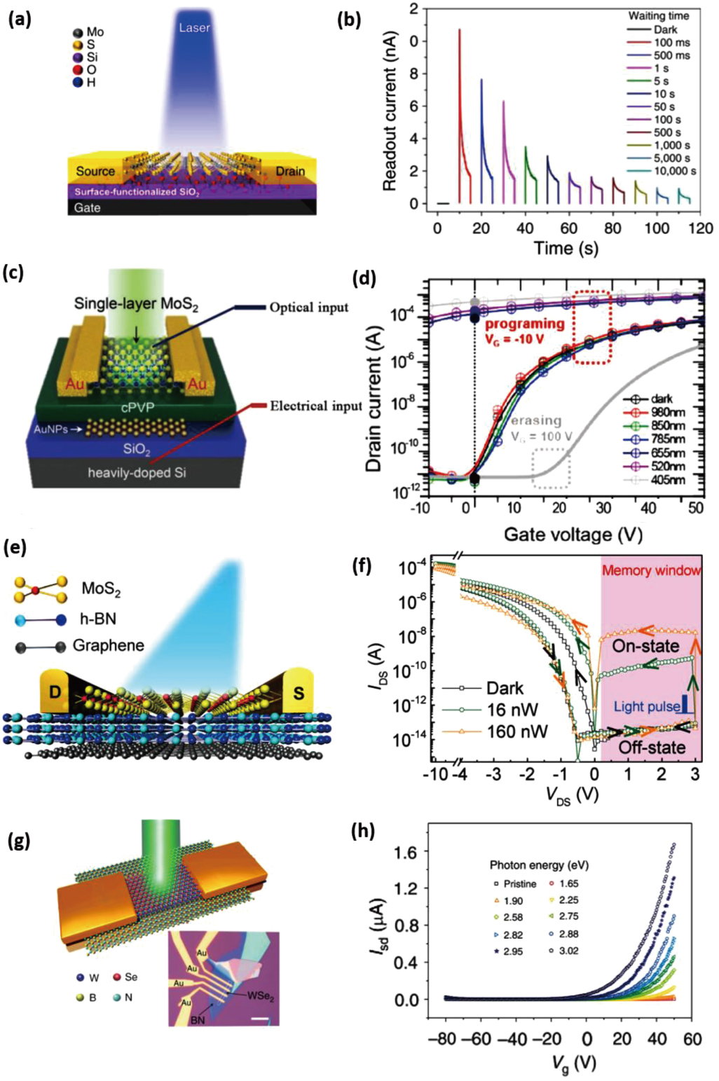
(a) Schematic diagram of an optoelectronic memristor based on silanol groups functionalized MoS2/SiO2 interface and (b) the relationship between read current and different light illumination durations.[70] Copyright (2017) Springer Nature. (c) The structure of single layer MoS2 based optoelectronic memory device and (d) the evolution of the device current upon photo illuminations with various wavelengths.[71] Copyright (2016) John Wiley & Sons, Inc. (e) Schematic structure of an optical memristor based on the heterojunction of the MoS2/h-BN/graphene, (f) The IDS–VDS curves of the device obtained with and without light pulses.[69] Copyright (2019) John Wiley & Sons, Inc. (g) Schematic illustration of the WSe2/BN heterostructure-based optoelectronic memory. Inset: optical image of the device. The scale bar is 10 μm. (h) Evolution of the device current obtained under illumination at various light intensities.[73] Copyright (2018) Springer Nature. |