Surface potential-based analytical model for InGaZnO thin-film transistors with independent dual-gates
He Yi-Ni, Deng Lian-Wen, Qin Ting, Liao Cong-Wei, Luo Heng, Huang Sheng-Xiang
School of Physics and Electronics, Central South University, Changsha 410083, China


† Corresponding author. E-mail: denglw@csu.edu.cn

Project supported by the National Key Research and Development Program of China (Grant No. 2017YFA0204600) and the Fundamental Research Funds for the Central Universities of Central South University, China (Grant No. 2019zzts424).

Abstract

An analytical drain current model on the basis of the surface potential is proposed for indium–gallium zinc oxide (InGaZnO) thin-film transistors (TFTs) with an independent dual-gate (IDG) structure. For a unified expression of carriers’ distribution for the sub-threshold region and the conduction region, the concept of equivalent flat-band voltage and the Lambert W function are introduced to solve the Poisson equation, and to derive the potential distribution of the active layer. In addition, the regional integration approach is used to develop a compact analytical current–voltage model. Although only two fitting parameters are required, a good agreement is obtained between the calculated results by the proposed model and the simulation results by TCAD. The proposed current–voltage model is then implemented by using Verilog-A for SPICE simulations of a dual-gate InGaZnO TFT integrated inverter circuit.

1. Introduction

Amorphous indium–gallium zinc oxide thin film transistors (a-InGaZnO TFTs) are advantageous for the next-generation display, due to the merits of high driving ability, good reliability, and mature process over large fabrication areas.[15] To further extend the applications of InGaZnO TFTs, the independent dual-gate structure is preferably adopted to adjust the threshold voltage in a wider range. Dual-gate InGaZnO TFTs render circuit response fast and power consumption low.[68] Previous researches show that the threshold voltage of the driving transistor can be adjusted dynamically by discharging the auxiliary gate, which benefits good compensation effect for active matrix organic light emitting diode (AMOLED) displays.[9] In the case of system-on-panel circuit integrations, it was proposed that high voltage–gain amplifiers be replaced by the dual-gate InGaZnO TFTs with differential inputs.[10] Although some dual-gate InGaZnO TFT circuits were implemented and measured, there have been no mature analytical current–voltage models for dual-gate InGaZnO TFTs up to date, which brings the difficulties in designing TFTs circuit by using SPICE tools.

SPICE simulations require an analytical TFT model, which is efficient and timing saving, compared with numerical calculations.[11,12] In recent years, the lack of appropriate analytical current–voltage model for InGaZnO TFTs attracts widespread attention from academic and industry. Perumal et al.[13] presented a compact model of InGaZnO TFTs on the basis of metal–oxide–semiconductor field-effect transistor (MOSFET) SPICE model. But the model is not accurate enough. Tsuji et al.[14] developed an efficient model for numerical simulations of single-gate InGaZnO TFTs. Cai et al.[15] successfully developed a drain current–voltage model for dual-gate InGaZnO TFTs, which is suitable for sub-threshold and above-threshold operating regions. However, the presented model is strongly dependent on the pre-determined threshold voltage, which is also difficult to calculate from physical parameters.

In this paper, an analytical current model is developed for independent dual-gate (IDG) InGaZnO TFTs on the basis of the surface potential. The effective carrier density is introduced and the Lambert function is used to solve the Poisson equation. It was proposed that the equivalent flat band voltage, i.e., VFB, can be used to characterize the phenomenon that the sub-threshold potential of the device is linearly modulated by the top gate voltage, i.e., VGT. In addition, the Lambert function is simplified by solving the potential of the sub-threshold region and the conduction region, separately. On the basis of the derived surface potential, the current–voltage expression can be derived by solving the dual integration of Pao–Sah’s law. The proposed current–voltage model is applied to the SPICE simulation and validated effectively.

2. Surface potential model for IDG InGaZnO TFTs

Figure 1 shows the cross sectional view of InGaZnO TFT with independent dual-gates. The direction parallel and perpendicular to the TFT channel are defined as the y direction and x direction, respectively. Here tIGZO, tOXF, and tOXB are the thickness of the InGaZnO layer, the top, and bottom gate dielectric layer, respectively. For the IDG InGaZnO TFT, the top gate voltage (VGT) and bottom gate voltage (VGB) are biased independently. For the simplicity of calculations, in this investigation, geometrical parameters for the top gate and bottom gate are the same, i.e., thicknesses of the metal and gate insulating layer are identical.

Fig. 1. The cross sectional view of independent biased dual-gate InGaZnO TFTs.

As an amorphous N-type semiconductor material, intrinsically, InGaZnO has a surface potential dependent on free electrons and localized electrons. Hence the potential of InGaZnO film follows the Poisson’s equation

where φ is the potential along the x direction, q is the electrical charge of a single electron, ρ is the volume charge density, and εIGZO is the permittivity of the InGaZnO film.

Using the Boltzmann distribution function, the effective carrier density can be expressed as[16]

where NEFF is the effective carrier density, kTEFF is the characteristic energy, and φ, VCH, and φF0 are the electrostatic potential, the channel voltage in the y direction, and the equivalent Fermi potential, respectively.

Due to the fact that

through solving Eq. (1), the electric field at the surface of the InGaZnO layer, i.e., EIGZO, can be expressed as

where φS is the surface potential.

For the interface between the gate-insulator and the InGaZnO layer, the Gaussian law can be used to relate the top and bottom gate voltage and the boundary electrical field together. Consequently, it can be derived that

where VFB is the flat-band voltage, Cox is the oxide capacitance per unit area, and φT is the surface potential near the top gate. Combining Eqs. (3) and (4b), by the integration method, one can obtain that

However, equation (5) shows an implicit function of φS, which is not straightforward for calculations. Here the Lambert-W function is used, where ω = W(x) is the solution of the transcendental equation ω·exp(x) = x. Thus, the solution of Eq. (5) can be obtained as

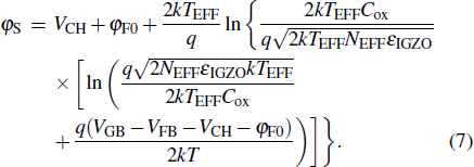
But the Lambert-W function cannot be embedded into SPICE simulations.[17] According to the actually operating conditions of the IDG InGaZnO TFTs, it is possible to simplify Eq. (6). For the conduction region (VGBVFBφF0 > VCH), the exponential term in the W function increases rapidly. Then using the approximation that W(x) = ln(x) − ln(ln x),[18] φS can be expressed as

On the other hand, for the sub-threshold region (VGBVFBφF0 < VCH), the exponential term in the W function approaches to 0. In addition, due to the observed linear relationship between φS and the top gate bias voltage VGT, φS can be expressed as

where λ depends on the ratio of the equivalent capacitance of the gate oxide layer to that of the active layer, which represents the modulation extent of VGB for φS; VFB is the equivalent flat band voltage, which can be divided into VFB1 and VFB2. Here VFB1 represents the difference in work function between the gate metal and InGaZnO layer, and VFB2 denotes the influence of the oxide layer and interface charge. As the carrier concentration of InGaZnO layer is modulated by VGT, the VFB can be expressed as

For a continuous expression of surface positional for IDG InGaZnO TFT with different operating regimes, equations (8) and (9) can be combined through a smoothing function of tanh x, then φS is expressed as

3. Drain current model of IDG InGaZnO TFT

On the basis of the obtained analytical surface potential, the current–voltage model for IDG InGaZnO TFT is developed as follows. According to the Pao–Sah formula, the drain–source current of the IDG InGaZnO TFT is

where μEFF is the effective mobility, W and L represent the width and length of the TFT. According to the previous investigations, the stretch-exponential function is consistent well with the curves of measured effective mobility versus gate–source voltage, thus

where m is the shape fitting parameter for the curve of mobility versus VGB.

Then the partial derivative of E (Eq. (3)) with respect to the channel voltage (i.e., VCH) is given as

Substituting Eqs. (12) and (13) into Eq. (11), one can obtain

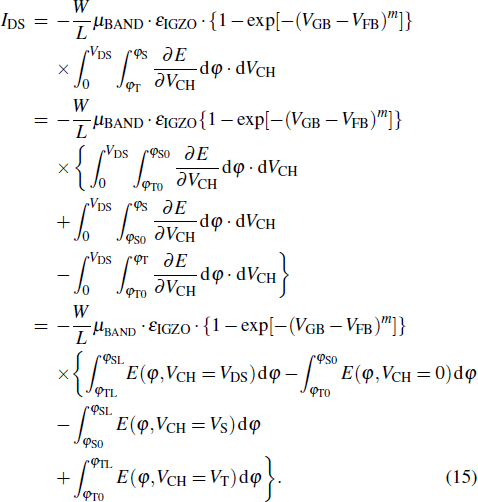
Figure 2 demonstrates the comparison of the TCAD simulated and calculated φS and φT versus channel voltage, from VCH = 0 to VCH = VDS. It is observed that the calculated and the simulations results are in good agreement with each other. According to Eq. (14), figure 2 shows the integration boundaries. By dividing the integration regions, IDS can be derived as

Fig. 2. Plots of surface potential φS and top potential φT versus channel voltage for IDG InGaZnO TFT, with colored area referring to integration region.

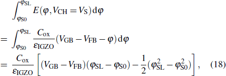
By directly integrating Eq. (3), the first and second terms on the right-hand side of Eq. (15) can be derived as

By combining Eq. (4a) and Eq. (4b), the third and fourth integral terms of Eq. (15) can be derived as

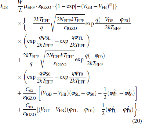
Consequently, the analytical expression for the IDS of IDG InGaZnO TFT is

4. Results and discussion

To verify the developed model, comparisons are carried out between the calculated and TCAD simulated results. The investigated TFT structure is shown in Fig. 1, and the VGT and the VGB are biased independently. Listed in Table 1 are the physical and geometrical parameters to calculate the current–voltage curve for IDG InGaZnO TFTs.

Table 1.

InGaZnO TFT parameters for TCAD simulation and model calculation.

.

Figure 3 shows the comparison between the calculated surface potential using Eq. (9) and the simulated surface potential. The potential of the sub-threshold region is shifted with VGT increasing, but the slope of sub-threshold surface potential remains unchanged approximately till VGT reaches to 0.5 V. Under various biasing conditions, the calculated values of φS in good agreement with the simulated ones.

Fig. 3. Simulated and calculated plots of surface potential φS versus bottom gate voltage VGB for three different values of VGT.

Figure 4 shows the comparison results of the simulated and calculated drain-source current versus VGB for different values of VGT. Further, the calculated and simulated output characteristics of IDG InGaZnO TFT are shown in Fig. 5. For both the transfer and output characteristics, the proposed model shows a high consistence with TCAD simulations, and the absolute error is less than 10−8. It is demonstrated that the threshold voltage of InGaZnO TFT can be adjusted using the independent biased gate electrode. With the decrease of VGT, the threshold voltage shifts positively, because more charges in the InGaZnO film are depleted.

Fig. 4. Comparison between simulated and calculated transfer characteristics of IDG a-InGaZnO TFT for three different values of VGT.
Fig. 5. Comparison between calculated and simulated output characteristics of IDG a-InGaZnO TFT with VGT = −5 V for various values of VGS.

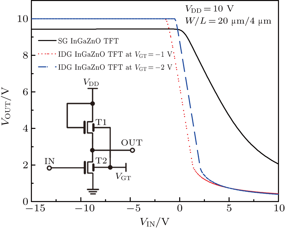
The proposed model is integrated into circuit simulations with Verilog-A. Figure 6 shows the HSPICE simulation comparison results of an InGaZnO TFT inverter with single-gate (SG) and independent dual-gate (IDG). The power supply (VDD) is 10 V, and VGT for the IDG transistor is −1 V and −2 V, respectively. It is observed that increased output swing and narrower transient region can be obtained by the IDG transistors.

Fig. 6. Comparison results between SG and IDG InGaZnO TFTs using Verilog-A model, with inset schematically showing inverter circuit with IDG InGaZnO TFTs.
5. Conclusions

In this work, an analytical drain current model for independent dual-gate InGaZnO TFT is established based on the surface potential. Equivalent flat band voltage VFB is introduced to represent the linear surface potential modulation effect of the top gate voltage VGT. Following the Pao–Sah’s law, regional integration is carried out in detail to obtain a continuous current–voltage model for the independent dual-gate InGaZnO TFTs. Comparisons between the model calculations and the TCAD simulations are carried out, and the results show that both the transfer and output characteristics are in good agreement for different operation regions. Furthermore, in order to verify the effectiveness of IDG InGaZnO TFTs for high-performance circuit designs, the model is applied to an SPICE simulator using Verilog-A, which is helpful in designing the high performance InGaZnO TFT circuit for system on panel circuit integrations.

Reference
[1] FortunatoE BarquinhaP MartinsR 2012 Adv. Mater. 24 2945
[2] FengG D ZhaoY H JiangJ 2019 Solid State Electron. 153 16
[3] HuW N JiangJ XieD D WangS T BiK X DuanH G YangJ L HeJ 2018 Nanoscale 10 14893
[4] LanL F DaiX Q HeC C LiuL YangX B LiangL Y CaoH T PengJ B 2019 IEEE Trans. Electron Dev. 66 2620
[5] SongE L LanL F XiaoP LinZ G SunS LiY Z SongW GaoP X PengJ B 2016 IEEE Trans. Electron Dev. 63 1916
[6] QinT HuangS X LiaoC W YuT B LuoH LiuS DengL W 2018 Acta Phys. Sin. 66 097101 in Chinese
[7] ZanH W LiC H YehC C 2011 Appl. Phys. Lett. 98 253503
[8] QinT LiaoC W HuangS X YuT B DengL W 2018 Jpn. J. Appl. Phys. 57 014301
[9] ZaidiW CostaJ PouryazdanA AbdullahW MünzenriederN 2018 IEEE Electron Dev. Lett. 39 1314
[10] TaiY H ChiuH L ChouL S ChangC H 2012 IEEE Electron Dev. Lett. 33 1729
[11] ParkJ H LeeS JeonK KimS KimS ParkJ SongI KimC J ParkY KimD M KimD H 2009 IEEE Electron Dev. Lett. 30 1069
[12] JeonK KimC J SongI ParkJ KimS KimS ParkY ParkJ H LeeS KimD M KimD H 2008 Appl. Phys. Lett. 93 182102
[13] PerumalC IshidaK ShabanpourR BoroujeniB K PettiL MünzenriederN SalvatoreG A CartaC TrösterG EllingerF 2013 IEEE Electron Dev. Lett. 34 1391
[14] TsujiH NakataM SatoH NakajimaY FujisakiY TakeiT FujikakeH YamamotoT ShimidzuN 2014 J. Disp. Technol. 10 101
[15] CaiM X YaoR H 2018 Sci. Chin. (Inf. Sci.) 61 022401
[16] QinT HuangS X LiaoC W YuT B DengL W 2017 Acta Phys. Sin. 57 014301 in Chinese
[17] AlvaradoJ IñiguezB EstradaM FlandreD CerdeiraA 2010 Int. J. Number. Model. Electron. Netw. Dev. Fields 23 88
[18] HoorfarA HassaniM 2008 J. Inequalities Pure Appl. Math. 9 5