Irradiation hardening behaviors of tungsten–potassium alloy studied by accelerated 3-MeVW2+ ions
Yang Xiao-Liang1, 2, Chen Long-Qing1, Qiu Wen-Bin1, Song Yang-Yi-Peng1, Tang Yi1, Cui Xu-Dong2, †, Liu Chang-Song3, Jiang Yan3, Zhang Tao3, Tang Jun1, ‡
Key Laboratory of Radiation Physics and Technology of Ministry of Education, Institute of Nuclear Science and Technology, Sichuan University, Chengdu 610064, China
Sichuan Research Center of New Materials, Institute of Chemical Materials, China Academy of Engineering Physics, Mianyang 621999, China
Key Laboratory of Materials Physics, Institute of Solid State Physics, Chinese Academy of Sciences, Hefei 230031, China


† Corresponding author. E-mail: xudcui@caep.cn tangjun@scu.edu.cn

Project supported by the National Natural Science Foundation of China (Grant Nos. 11975160, 11775149, and 11475118) and the International Thermonuclear Experimental Reactor (ITER) Program Special, China (Grant No. 2011GB108005).

Abstract

Tungsten–potassium (WK) alloy with ultrafine/fine grains and nano-K bubbles is fabricated through spark plasma sintering (SPS) and rolling process. In this study, 3-MeV W2+ ion irradiation with a tandem accelerator is adopted to simulate the displacement damage caused by neutrons. As the depth of irradiation damage layer is limited to only 500 nm, the hardening behaviors of WK alloy and ITER (International Thermonuclear Experimental Reactor)-W under several damage levels are investigated through Bercovich tip nanoindentation test and other morphological characterizations. The indenter size effect (ISE), soft substrate effect (SSE), and damage gradient effect (DGE) are found to influence the measurement of nano-hardness. Few or no pop-ins in irradiated samples are observed while visible pop-in events take place in unirradiated metals. Extensive pile-up with different morphology features around the indentation exists in both WK and ITER-W. The WK shows a smaller hardness increment than ITER-W under the same condition of displacement damage. This study provides beneficial information for WK alloy serving as a promising plasma facing materials (PFMs) candidate.

1. Introduction

International Thermonuclear Experimental Reactor (ITER) is a meaningful way to solve the current energy crisis considering fossil energy consumption and intractable long-lived radioactive waste in the nuclear fission industry.[1] However, the core materials in ITER usually serve in complex environments, especially the plasma facing materials (PFMs) which are always subjected to thermal shock, plasma irradiation, and neutron irradiation.[25] Therefore, the development of PFMs with excellent performance is the prerequisite for the ITER project. Tungsten (W) is expected to be one of the most promising candidates serving as PFMs in ITER due to the high level of melting point (∼ 3420 °C), density (∼ 19.25 g/cm3), thermal conductivity (∼ 170 W/m⋅K), high-temperature strength, sputtering thresholds, and irradiation resistance.[6]

Despite these intrinsic advantages mentioned above, W needs to be further investigated in order to meet specific requirements in engineering. The WK alloy (potassium-doped tungsten/K-bubble W) was initially developed from the electric filament industry. The researches of Coolidge (powder metallurgy tungsten processing, 1909), Pacz (the non-sagging tungsten, 1917), and Tury (the AKS-doping of tungsten, 1931) all played a great promotion role in developing the K-doped W. The strengthening mechanism of non-sagging tungsten (potassium bubble strengthening) was not verified by Wronski et al. until the 1960’s.[7,8] Tungsten–potassium (WK) alloy has proved to be another potential candidate for PFMs, due to its excellent mechanical properties, high thermal shock resistance, and low hydrogen retention. In general, the displacement damage of PFMs caused by high energy particles in fusion reactor is of major concern in engineering requirements. Especially, irradiation hardening of W alloys in PFM’s service conditions (including 14-MeV neutron irradiation) is one of the most critical issues of degradation in nuclear fusion materials. Moreover, tungsten will mainly transmute to rhenium, osmium, etc. by neuron bombardment in the fusion environment. This change of composition will cause detrimental or beneficial influence on W-based PFMs. Additionally, the light-nuclei elements produced in transmutation can introduce extra brittleness. Displacement damage and transmutation induced by neutron both have an important influence on material properties. It has been shown that the neutron-irradiated W and tungsten–rhenium alloy exhibit substantial irradiation hardening. It was also confirmed that the dominant irradiation defects such as dislocation loops and small clusters will evolve into single-crystal bulk W and polycrystalline W foils during neutron irradiation.[3,5,912]

However, since high neutron doses are very time-consuming (a few displacements per atom per year), ion irradiations are usually utilized to simulate the displacement damage of neutrons. In the 1980s, Zinkle published the first paper about the study of the irradiation hardening behaviors of nuclear materials through ion irradiations and nanoindentation tests.[13] The depth-dependence in the hardness on ion-irradiated steels was investigated by nanoindentation tests through continuous stiffness measurement (CSM). The relations between the damaged microstructure of W-based alloys and parameters of self-ion irradiation were reported in the previous investigations.[1416] Most of these obtained results focused on the depth-dependence or damage to microstructure of irradiation in tungsten or ferritic alloys, but little attention was paid to the comparison of hardening behaviors between ITER-W (tungsten materials which meet the specification defined by ITER Organization) and WK alloy irradiated by self-ions. Our previous studies have discussed the design of doping phases and SPS preparation process optimizations.[17,18]

Here in this work, SPSed WK alloy is further rolled to improve its mechanical properties. We study the irradiation hardening behaviors of WK alloy and ITER-W irradiated by 3-MeV W2+ ions through nanoindentation technique because the depth of irradiation damage is usually limited in the order of micron meters. Hardening data obtained from a CSM nanoindentation technique with Berkovich pyramidal tips are analyzed and discussed in detail. Moreover, the pop-in events and pile-up phenomena as a function of ion dose are investigated as well.

2. Materials and methods
2.1. Preparation of WK alloy

Commercial AKS (Al–K–Si)-doped tungsten powder (purity > 99.9%, average particle size 3.28 μm, Zigong Cemented Carbide Corporation) was used as raw material. Firstly, the prepared powder was pre-compacted at 80 MPa to form a block in a graphite die. Then the following sintering process was carried out in sequence: the entire graphite die was moved into an SPS chamber and heated up to 1750 °C at a heating rate of 100 °C/min. After being maintained for 3 min, the system was self-cooled to the room temperature inside the chamber. The detailed sintering parameters can be found elsewhere.[17,18] After sintering, the WK bulk with relative density > 97% was multi-pass continuously rolled with a deformation rate of up to 80%. The consolidated ingot with relative density ∼ 100% and average grain size 35 μm was cut into plates with 15 mm in diameter and 2 mm in thickness for irradiation experiments and various characterizations. All plate samples were mirror polished and annealed in a vacuum furnace at 1473 K for 2 h prior to irradiation experiments.

2.2. W2+ ion irradiation

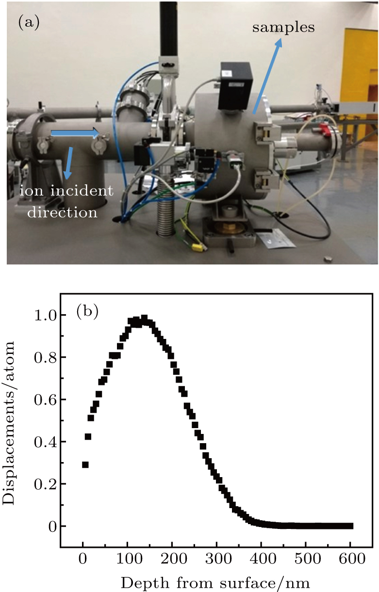
The 3-MeV W2+ ions were used for the self-ion irradiation in a tandem accelerator (Fig. 1(a)) located at Sichuan University, China.[19] The software “Stopping Range of Ions in Matter” (SRIM) was used to simulate the irradiation results and calculate the projected ranges (approximately 200 nm) in bulk samples. A typical displacement damage profile calculated by SRIM-2008 is shown in Fig. 1(b). Full damage cascade code and the threshold displacement energy of 90 eV for tungsten were used in the calculation process.[20] The maximum damage depth was about 500 nm with peak damage at 140 nm. The peak damage rate was 2.77 × 10⁻⁴ dpa/s and the total displacement damages reached up to 2 dpa, 5 dpa, and 8 dpa, respectively. The irradiation temperature was controlled at 650 °C within an error of ±10 °C, the incident angle was set to be 0° (perpendicular to rolling direction), and the fluence rate was about 1 × 10¹⁴ (ion/cm2)/h. In this research, 0 dpa represented the unirradiated case and the ITER-W (average grain size 33 μm) counterparts were supplied by Xiamen Tungsten Corporation.

Fig. 1. (a) Tandem accelerator terminal in Sichuan University, and (b) depth profile of displacement damage under self-ion irradiation of pure W (by SRIM).
2.3. Nanoindentation test

The nanoindentation tests were performed in EMS-60 (Agilent Technologies), and the depth (h)–hardness (H) profiles were obtained through CSM. In the CSM, a small sinusoidal oscillation in the load signal was used to measure stiffness dynamically during the indentation sequence, and the corresponding displacement signal was monitored. The 2-nm displacement amplitude, 45-Hz constant loading rate, 0.05-s−1 strain rate, and a maximum indentation depth of 2 μm were set for all Berkovich indentations. The Berkovich indenter was more readily fashioned to a sharper point than the four-sided Vickers geometry, thus ensuring a more precise control over the indentation process. The Oliver–Pharr method was used to calculate hardness and calibrate the blunting of the indentation tip. Traditional XRD (DX2700, Haoyuan, China) tests at an acceleration voltage 50 kV, operating current 150 mA, and a step width 0.02°, AFM (Edge, Bruker, USA) tests with standard probe in tapping mode, and SEM (S4800, Hitachi, Japan) characterizations with acceleration voltage 15 kV–20 kV were also utilized in this work.

3. Results and discussion
3.1. Nanoindentation

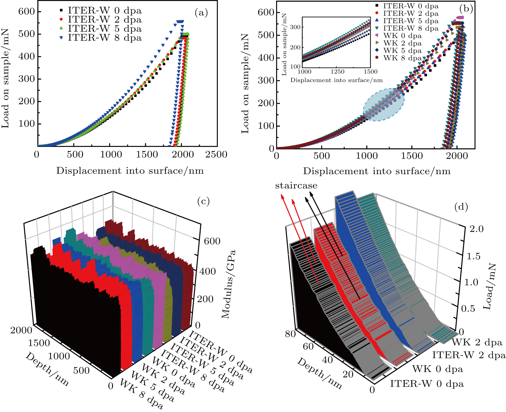
The representative load–depths and modulus–depths of samples after irradiation damage in the nanoindentation test are displayed in Fig. 2. Generally speaking, in Fig. 2(a), the load for the irradiated ITER-W alloy rises faster than that for the unirradiated specimen with the same indentation depth. Figure 2(b) exhibits the common load–displacement profiles for all 8 samples. The loads on the WK alloy surface show different patterns: slightly larger load for unirradiated (also called 0 dpa) WK alloy than that of ITER-W, but larger scattered data under the same conditions. The plasticity indexes (=plastic work/total work ≈hresidual/hmax)[21] span a very narrow range from 0.915 to 0.936, which means that both WK and ITER-W show similar plasticity at room temperature. The initial slopes of the unloading curves are found to be almost parallel to each other, indicating almost identical elastic modulus in the specimens. Figure 2(c) shows the indentation modulus as a function of depth for each dose. The average modulus is 450 GPa with no significant variation. The slight increment of measured modulus at smaller indentation depth is thought to be due to the slight bluntness of the indenter tip.[22] It should be noted that some sudden jumps in displacement are observed in these tests of unirradiated WK and ITER-W samples as depicted in Fig. 2(d). Discrete jumps in tip displacement known as pop-in (“staircase”) events are produced mainly by the nucleation of the initially formed dislocations, relieving strain beneath the tip. A general understanding of pop-in events during nanoindentation in metals is that they are related to activating dislocation source in a probed material volume. In the irradiated material, there are plenty of irradiation-induced defects (such as dislocation loops) which can easily activate dislocation sources, reduces or even eliminates the need to arouse a dislocation source. Similar phenomena have been reported by many indentation studies on ion-irradiated materials.[10,23] Thus, it well explains the fact that there are practically few or no pop-ins in the irradiated damage 2 dpa, while here exist several pop-in events in unirradiated samples.

Fig. 2. (a) Typical load–displacement profiles for ITER-W specimens, (b) representative load–displacement profiles for all 8 samples, (c) similar modulus–depth profiles for WK alloy and ITER-W, and (d) discrete displacement jumps in depth below 80 nm for WK 0 dap, WK 2 dpa, ITER-W 0 dpa, and ITER-W 2 dpa.

Figure 3(a) displays the depth profiles of hardness in self-ion irradiated samples. Each sample has ten indentations in a straight line, with spacing of 40 μm to avoid the deformation overlap. The inset in Fig. 3(a) shows the morphology of ITER-W 8 dpa indentation captured by an optical microscope. Other ITER-W or WK sample has a similar triangular shape of indentation. From Fig. 3(a) we notice that for both unirradiated and irradiated samples, hardness decreases clearly with indent depth increasing. This phenomenon is observed at an indentation depth of h > 100 nm. Such a depth-dependent hardness behavior can be ascribed to an indentation size effect (ISE). In contrast, for the initial dozens of nanometers, hardness increases with depth increasing, which is known as reverse ISE. The reverse ISE is usually attributed to testing artifacts, so we will not use the hardness data at h < 100 nm for further discussion in this paper.

Fig. 3. (a) Depth profiles of hardness for ITER-W and WK alloys after 3-MeV W2+ ion irradiation at 650 °C, with inset showing optical micrograph of nanoindentation in ITER-W after 8-dpa damage. Plots of (c) hardness and (d) hardness increment versus damage to irradiated layers in WK and ITER-W samples.

Another significant softer substrate effect (SSE) refers to the fact that the contribution from beyond the harder ion-irradiated surface should not be neglected because the substrate begins to plastically deform before the indenter tip reaches the substrate. This kind of SSE has been seen in various systems of a hard thin film on a soft substrate.[22,2428] It is widely believed that an indentation depth of less than 10% of the coating allows the coating properties to be measured without influence from the substrate. However for the self-ion irradiated layer, the data from 0-nm depth to 100-nm depth are heavily influenced by surface roughness, tip blunting or initial pop-ins (below approximately 80 nm in depth). The average hardness values from 100 nm to 200 nm are considered to be the implanted layer hardness. Figure 3(c) shows the plots of hardness versus damage of the irradiated layer in WK and ITER-W samples. The hardness of unirradiated pure W is 5.95 GPa. At a damage level of 2 dpa, hardness significantly is raised to 8.92 GPa. Moreover, the hardness increases to 9.16 GPa at 5 dpa, and 9.60 GPa at 8 dpa. For the case of WK alloy, the initial hardness, 6.27 GPa, is higher than that of ITER-W, with an increment in hardness at 2 dpa of 2.01 GPa (from 6.27 GPa to 8.28 GPa). A similar increase also happens at 5 dpa (from 8.28 to 8.98 GPa). Finally, there is a little increment in hardness up to 9.29 GPa at 8 dpa. The hardness increment slows down until the damage reaches 8 dpa with a tendency of harden saturation. The dose dependence for these alloys in the present study follows a power-law ΔH ∝ (dpa)n,[29] then n = 0.29 for ITER-W and n = 0.15 for WK are obtained (ΔH is the amount of irradiation hardening). Supposing that the number density of obstacles increases linearly with displacement damage, the dose dependence can be modeled by the power-law with n = 0.5. The smaller n values for WK and higher for ITER-W are probably due to the defects of saturation at higher dose.[22,30]

3.2. Irradiation hardening

It is generally recognized that the hardness depth profile after self-ion irradiation can intrinsically include mainly three different dependent effects: ISE, SSE, and DGE.[24] In order to explain ISE, Nix and Gao[24] developed a model (Nix–Gao model) based on a concept of geometrically necessary dislocation. The Nix–Gao model gave the relation between infinite depth hardness (H0) and the hardness (H) of measured depth (h) as follows: H = H0(1 + (h*/h))0.5, where h* is a characteristic length dependent on material and indenter shape. Our hardness data are plotted as H2 versus 1/h as shown in Fig. 4(a). The value of H0 is calculated by the least square fitting of hardness data in a range of 100 nm < h < 500 nm which includes most part of the irradiated region. The plots for unirradiated (0 dpa) ITER-W and WK are quite similar to each other, and the unirradiated samples show good linear relation in a range of h > 100 nm. Comparing with the unirradiated samples, the hardness for self-ion irradiated sample clearly increases with depth increasing. Such irradiation hardening behaviors of the ion irradiated materials can also be seen in the literature. Over a certain indentation depth, the contribution of the softer unirradiated region (substrate) below the harder ion-irradiated surface to the hardness should not be ignored with indent depth increasing. As a result, the curve of H2 versus 1/h in 8-dpa sample presents two different slopes of the line while the unirradiated samples each show only one. For 2-dpa and 5-dpa samples, similar response curves fell in a range between 0 dpa and 8 dpa. The curve of H0 value and hardening versus displacement damage from the Nix–Gao model are exhibited in Fig. 4(b) and its inset, respectively. Though WK presents higher initial hardness than that of ITER-W without irradiation, the hardness increment of WK decreases more slowly. When the damage level reaches 8 dpa, the ITER-W shows a much higher hardness than the WK.

Fig. 4. Plots of H2 versus 1/h for ITER-W/WK before and after self-ion irradiation, with different slopes indicating irradiated layer and undamaged layer. (b) H0 value of WK/IETER-W versus displacement damage. Inset shows irradiation hardening versus displacement damage.

A remained problem to model the depth–profile of hardness in the irradiated materials is the damage gradient effect (DGE). The SRIM result from Fig. 1(b) clearly shows the peak displacement damage at a depth of about 140 nm, indicating that there exists a DGE in this case. However, in the present study, neither the ITER-W nor WK shows evident fluctuations or peaks of hardness in this damage gradient region. This unconformity is probably due to the fact that the ISE and SSE are too distinct to cover up DGE. As far as we know, the irradiation hardening of W materials depends strongly on the original composition and irradiation condition. As the irradiation conditions of both materials are the same, the only reason for hardening difference is the composition and microstructure between ITER-W and WK. On the one hand, the potassium bubbles become liquid under the high-temperature irradiation so that the pressure of K bubbles increases.[31] It will cause the tungsten lattice to distort, and increase the resistance of tungsten self-interstitial atoms or the vacancy movement during the cascade. On the other hand, although the grain sizes of ITER-W and WK are basically identical, potassium bubbles, especially those on the grain boundaries, create additional interfaces, which will absorb the point defects generated in the irradiation process.[32,33] It also weakens the generation of dislocation loops or voids.

3.3. XRD, AFM, and SEM

The hardening behaviors of ITER-W and WK self-ion-implanted at 650 °C are characterized by XRD and AFM. The XRD patterns in Fig. 5(a) are matched with the PDF data bank to track the evolution of phases during irradiation. There are no apparent changes in grain size nor γ -W phase appearing.[33] However, the small changes of the relative peak positions may be attributed to macro-strain as figure 5(b) shows. After being irradiated by 8 × 10¹⁴-ion/cm2 W2+ at 650 °C, surface strain about 10−4 on the order of magnitudes is induced by using the Williamson and Hall method. The effect of irradiation-induced stress on nanoindentation hardness measurement needs further studying.
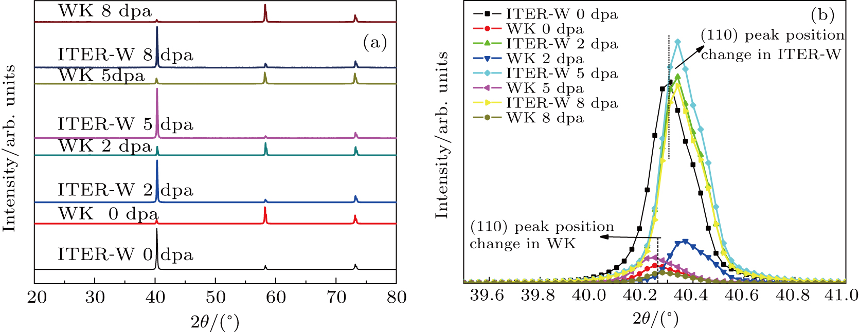
Fig. 5. XRD patterns of WK/ITER-W samples after different dose self-ion irradiations at different doses.

Sink-in or pile-up phenomenon of material in the vicinity of the indenter tip is characterized by using AFM, and the results are shown in Fig. 6. Figure 6(a) shows the indenter two-dimensional (2D) morphology of the WK/ITER-W samples. Figure 6(b) displays the detailed three-dimensional (3D) indentation morphology image of the WK 0 dpa while figure 6(c) exhibits the 2D image. The three straight lines and the colored marks in Fig. 6(c) denote the pile-up zone of nanoindentation. The imprint profiles as shown in Fig. 6(d) display the matched plasticity index mentioned above. There are small changes in both the height and the lateral extent of the pile-up with the increase of irradiation influence. Roughly speaking, the pile-up is clearly observed in the 2D AFM image of indentations; as the damage increases to 2 dpa, a noticeable pile-up height increases and subsequently decreases. The maximum values of ITER-W/WK are 2.7 μm/2.3 μm, 3.0 μm/2.9 μm, 2.5 μm/2.7 μm, and 2.5 μm/2.3 μm for 0 dpa, 2 dpa, 5 dpa, and 8 dpa, respectively. Some finite element simulations indicate that for large pile-ups, the areas deduced from the load–displacement curves will underestimate the true contact areas and lead the hardness and modulus to be overestimated. This argument verifies that the measured modulus is a bit larger than that from the W theory, 410 GPa. The extent of pile-up is related to the plastic deformation proximity of the indenter tip. Different sink-in/pile-up properties between irradiated and unirradiated materials are likely to obscure the observation of irradiation-induced changes in mechanical properties.[22] For indents in bulk materials, this behavior is dependent on the ratio of elastic modulus to yield stress, and the work-hardening coefficient.[34] The substrate beneath thin damage layer produced by ion implantation can also influence the sink-in/pile-up behavior during indentation.

Fig. 6. (a) AFM images to investigate WK and ITER-W pile-up, (b) 3D AFM image of nanoindentation from WK 0 dpa, (c) 2D image of nanoindentation from WK 0 dpa, and (d) indentation profiles of WK 0 dpa.

The SEM micrographs of fracture and surface of some samples are shown in Fig. 7. Some grain/sub-grain boundaries are revealed by sputtering or corrosion, but the ITER-W 5-dpa samples show equiaxed grains (Fig. 7(a)) while the long and thin grain/sub-grain boundaries exist in rolled WK alloy after 5-dpa damage (Fig. 7(b)). The preferred orientation of grains as shown by XRD results could explain the difference in surface morphology. For the unirradiated samples, the insets show clean and smooth surface without sub-grain boundaries. Massive inter- and intra-granular K bubbles formed in WK alloy (Fig. 7(c)) which is annealed at 1800 °C for 2 h as in our previous work.[18] Because of the quick sintering process, it is difficult for some K bubbles to migrate to grain boundaries. Hence, both intra and inter K bubbles serve as pinning centers in W which improves the mechanical properties.

Fig. 7. (a) Surface morphology of ITER-W 5 dpa with inset showing the scenario of unirradiated ITER-W, (b) surface morphology of WK 5 dpa with inset showing the scenario of unirradiated WK, and (c) fracture morphology of annealed WK.
4. Conclusions

In this work, we propose a new approach to the manufacturing of the WK alloy through SPS and rolling process which provides a better irradiation hardening resistance. Some conclusions can be drawn from the present study.

(i) Almost the same pop-in phenomena exist in unirradiated WK/ITER-W samples. Pile-ups exist in both WK and ITER-W samples, no matter whether the irradiation treatment is implemented. The ITER-W presents a similar plastic deformation to the WK alloy at room temperature.

(ii) Intrinsic ISE in ITER-W is different from that in WK, which influences the hardness depth profile after self-ion irradiation. The SSE can be identified through the Nix–Mao model while the effect of DGE on hardness is inconspicuous and hard to eliminate.

(iii) Despite a higher initial hardness value, the WK has a smaller hardness increment than the ITER-W under the same displacement damage. This is due to the suppression of irradiation defects by potassium bubbles. On the one hand, potassium bubbles increase the resistance to the development of irradiation-induced voids during high-temperature irradiation. On the other hand, the extra interface between the potassium bubbles and the tungsten grains can absorb the point defects induced by the cascade process.

Reference
[1] J H 2007 Fusion reactor materials Beijing Chemical Industry Press 25
[2] Knaster J Moeslang A Muroga T 2016 Nat. Phys. 12 424
[3] Ueda Y Coenen J W De Temmerman G Doerner R P Linke J Philipps V Tsitrone E 2014 Fusion Eng. Des. 89 901
[4] Zinkle S J Snead L L 2014 Annu. Rev. Mater. Res. 44 241
[5] Roth J Tsitrone E Loarte A Loarer T Counsell G Neu R Philipps V Brezinsek S Lehnen M Coad P Grisolia C Schmid K Krieger K Kallenbach A Lipschultz B Doerner R Causey R Alimov V Shu W Ogorodnikova O Kirschner A Federici G Kukushkin A 2009 J. Nucl. Mater. 390�?91 1
[6] Fu B Q Lai W S Yuan Y Xu H Y Li C Jia Y Z Liu W 2013 Chin. Phys. 22 126601
[7] Schade P 2010 Int. J. Refract. Met. Hard Mater. 28 648
[8] Yang X Qiu W Chen L Tang J 2019 Tungsten 1 141
[9] Platov Y M Lazorenko V M Tovtin V I Khasanov F A 2011 Inorg. Mater.: Appl. Res. 2 142
[10] Weaver J S Sun C Wang Y Kalidindi S R Doerner R P Mara N A Pathak S 2018 J. Mater. Sci. 53 5296
[11] Field K G Briggs S A Sridharan K Howard R H Yamamoto Y 2017 J. Nucl. Mater. 489 118
[12] Chen J Duan Y Yang Z Wang L Wu K Li K Ding F Mao H Xu J Gao W Zhang L Wu J Luo G N 2017 Chin. Phys. 26 095205
[13] Zinkle S J O W 1986 J. Nucl. Mater. 141 548
[14] Yi X Jenkins M L Hattar K Edmondson P D Roberts S G 2015 Acta Mater. 92 163
[15] Ogorodnikova O V Gasparyan Y Efimov V Ciupiński Ł Grzonka J 2014 J. Nucl. Mater. 451 379
[16] Zhang H Wen S L Pan M Huang Z Zhao Y Liu X Chen J M 2016 Chin. Phys. 25 056102
[17] Xiao Y Huang B He B Shi K Lian Y Liu X Tang J 2016 J. Alloys Compd. 678 533
[18] Huang B He B Xiao Y Ang R Yang J Liao J Yang Y Liu N Pan D Tang J 2016 Int. J. Refract. Met. Hard Mater. 54 335
[19] Han J An Z Zheng G Bai F Li Z Wang P Liao X Liu M Chen S Song M Zhang J 2018 Nucl. Instrum. Methods Phys. Res. Sect. B: Beam Interact. Mater. Atoms 418 68
[20] Stoller R E Toloczko M B Was G S Certain A G Dwaraknath S Garner F A 2013 Nucl. Instrum. Methods Phys. Res. Sect. B: Beam Interact. Mater. Atoms 310 75
[21] Beake B D Goel S 2018 Int. J. Refract. Met. Hard Mater. 75 63
[22] Armstrong D E J Wilkinson A J Roberts S G 2011 Phys. Scr. T145 014076
[23] Lorenz D Zeckzer A Hilpert U Grau P Johansen H Leipner H S 2003 Phys. Rev. 67 172101
[24] Kasada R Takayama Y Yabuuchi K Kimura A 2011 Fusion Eng. Des. 86 2658
[25] Hasegawa A Tanno T Nogami S Satou M 2011 J. Nucl. Mater. 417 491
[26] Bolshakov A Pharr G M 1998 J. Mater. Res. 13 1049
[27] Liu P P Wan F R Zhan Q 2015 Nucl. Instrum. Methods Phys. Res. Sect. B: Beam Interact. Mater. Atoms 342 13
[28] Wang Z Q Zhao Q Wei Y P et al. 2018 J. Alloys Compd. 732 406
[29] Takayama Y Kasada R Sakamoto Y Yabuuchi K Kimura A Ando M Hamaguchi D Tanigawa H 2013 J. Nucl. Mater. 442 S23
[30] Yabuuchi K Yano H Kasada R Kishimoto H Kimura A 2011 J. Nucl. Mater. 417 988
[31] Snow D 1972 Metall. Trans. 3 2375
[32] El-Atwani O et al. 2019 Acta Mater. 165 118
[33] Tan X Luo L Chen H Zhu X Zan X Luo G Chen J Li P Cheng J Liu D Wu Y 2015 Sci. Rep. 5 12755
[34] Zhang Z X Chen D S Han W T Kimura A 2015 Fusion Eng. Des. 98�?9 2103