|
Zhong Hai1, Sun Qin-Chao1, Li Guo1, Du Jian-Yu1, 2, Huang He-Yi1, 2, Guo Er-Jia1, 3, He Meng1, Wang Can1, 2, 4, Yang Guo-Zhen1, Ge Chen1, 2, †, Jin Kui-Juan1, 2, 4, ‡
|
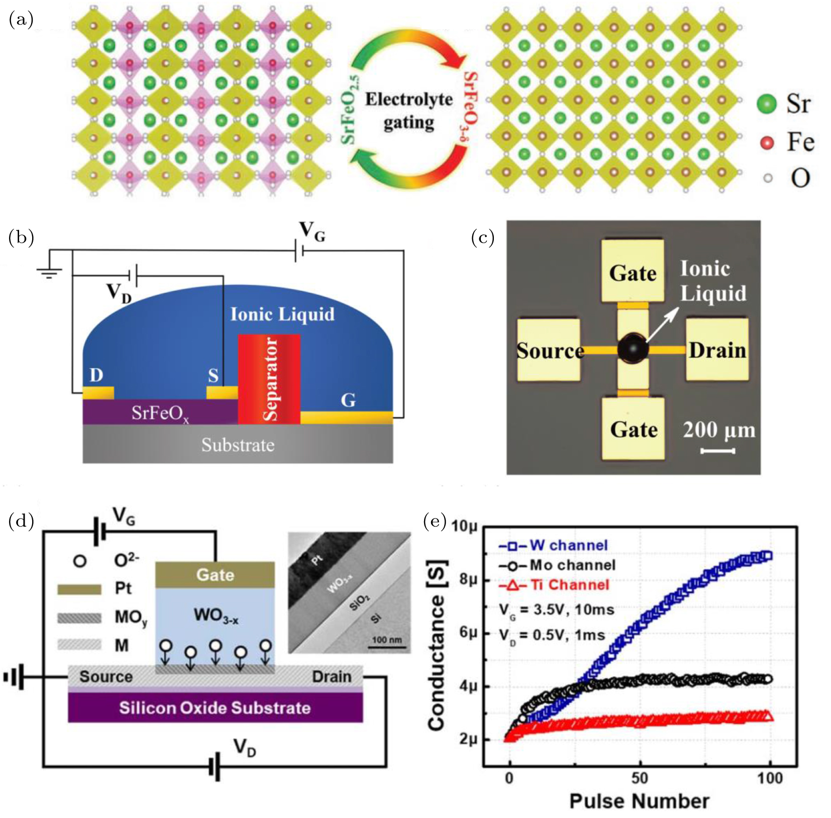
(a) Crystal structures of BM-SrFeO2.5 and PV-SrFeO3-δ thin films along the {100} direction on the SrTiO3 substrate. (b) Illustration of the transistor structure and measurement setup. (c) An optical image of a typical ferrite transistor device. Reprinted with permission from Ref. [75]. Copyright 2019, John Wiley & Sons. (d) Schematic diagram of the three-terminal synapse device structure, which includes the operating mechanism and measurement setup. Inset shows cross-sectional TEM image of Pt/WO3–x/W/SiO2/Si stack. (e) Channel conductance change (potentiation) for different channel metals as a function of positive gate pulses (3.5 V, 10 ms). Reprinted with permission from Ref. [86]. Copyright 2019, the Japan Society of Applied Physics. |