A compact electro-absorption modulator based on graphene photonic crystal fiber
Fu Guangwei, Wang Ying, Wang Bilin, Yang Kaili, Wang Xiaoyu, Fu Xinghu, Jin Wa, Bi Weihong
School of Information Science and Engineering, Key Laboratory for Special Fiber and Fiber Sensor of Hebei Province, Yanshan University, Qinhuangdao 066004, China


† Corresponding author. E-mail: earl@ysu.edu.cn whbi@ysu.edu.cn

Abstract

A compact electro-absorption modulator based on graphene photonic crystal fiber is proposed. To enhance the graphene–light interaction efficiency, the innermost six air-holes of photonic crystal fiber are replaced by two large semicircular holes, and monolayer graphene is deposited on the two large semicircular holes. By optimizing the structure parameters, a strong graphene–light interaction is obtained. Moreover, the switch on–off point of the modulator is unchangeable, which is only related to the frequency of the incident light. The influence factors of this composite structure have been analyzed. The proposed modulator is compared with other graphene-based modulators, and the results show that it is filled without dielectric spacer. There are some excellent performances, such as an extinction ratio 7 dB of y-polarization mode, 3-dB modulation bandwidth of 70 GHz with small footprint of 205 μm, and a consumption of energy per bit 59 pJ/bit.

1. Introduction

Optic modulator is a critical component in the optical fiber communication network, and its characteristics will directly affect the performance of transmission network. Graphene-based optic modulators have received extensive attention with the advent of graphene. At present, electro–optical modulator and all-optical modulator are mainly studied. All-optical modulator, a nonlinear optical process (such as two-photon absorption, saturable absorption, or nonlinear refraction) is required to realize control of light by light.[1] However, electro–optic modulations are easy to control and the materials are easy to access. In electro–optic modulation, the complex refractive index of materials will change due to the electro–optic effect when they are subjected to an external electric field, such as modulators based on semiconductor or LiNbO3,[2] but they suffer from a narrow operating bandwidth, which limits their further applications. Thereby a graphene-based electro–optic modulator (EOM) is proposed.

Graphene is a two-dimensional material formed by a single sheet of carbon atoms with a hexagonal lattice, which was found in 2004.[3] It has attracted enormous interests because of its unique electronic and optical properties, such as high carrier mobility,[4] absorption over a wide spectral range from visible to infrared.[5] Moreover, graphene is considered to be a perfect atomic monolayer with a rather unique band structure that the valence band and the conduction band touch each other at six points, which are called as the Diract points. The unique zero-gap bandstructure makes absorption in graphene easily controlled through doping or electrical gating by shifting the Femi level.[68] Those features above imply that graphene can be an appropriate candidate to be used as the active medium in electro–optical modulators. Recently the silicon waveguides and side-polished fibers integrated graphene-based electro–optic modulators have been demonstrated.[914] Compared with conventional modulators, EOM based on graphene has advantages of wide modulated bandwidth, low bias voltage, and small footprint. However, the waveguide integrated modulators suffer from high insertion loss, complex manufacturing process, which limit their applications in practice. Moreover, additional components in the fiber systems will increase optical transmission loss and system complexity. Besides, the side-polished fiber could destroy the structure of the optical fiber, resulting in additional energy loss via scattering effect, and the exposed core is easily affected by the ambient environment. To overcome above mentioned difficulties, photonic crystal fiber (PCF) can be used for EOM. PCF has the advantages of design flexibility, high confinement, controllable birefringence, etc.[15] Many functional devices based on PCF and graphene have attracted increasing attention, such as splitters,[16] all fiber laser,[17] refractive index sensor,[18] and so on. The performances of modulators based on PCF can be further promoted by growing uniform and large area graphene sheet into air holes. Direct graphene growth on silicon dioxide substrate by chemical vapor deposition (CVD) has been demonstrated.[19,20] In this way, graphene can be placing into the air holes of fiber instead of the chemical transfer method. The efficiency of electro–optic modulator can be enhanced by using PCF with additional electrodes to the optical fiber.

Taking the mentioned advantages of graphene and PCF, a compact electro-absorption modulator based on graphene photonic crystal fiber (G-PCF) is proposed. In order to enhance the light–matter interaction, the proposed PCF has two large semicircular holes, and a monolayer graphene is deposited on the curved holes in the center. In particular, the geometric parameters of PCF, the chemical potential of the graphene, and the frequency of the incident light related to the fundamental mode are investigated in detail using a two-dimensional finite element method (FEM). By optimizing these parameters, the electro-absorption modulator can reach to an extinction ratio of 7 dB in y-polarization mode, 3-dB modulation bandwidth of 70 GHz with small footprint of 205 μm, and a consumption of energy per bit of 59 pJ/bit.

2. Structure and principles of the G-PCF electro-absorption modulator
2.1. Structure of G-PCF

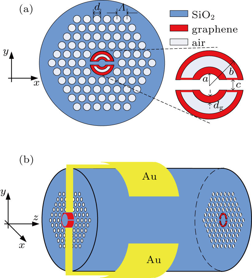
The proposed structure of the G-PCF is illustrated in Fig. 1.

Fig. 1. (a) Cross sectional view of G-PCF and (b) three-dimensional (3D) view.

In Fig. 1, the PCF consists of micro-structure of five-layer hexagonal concentric rings where the air holes are similar, but the innermost six air holes are replaced by two semicircular holes, which is aimed to generate refringence, and graphene is better coupled to a polarizing light of the fundamental mode. Two adjacent air-holes are placed with uniform distance Λ = 1.5 μm, and the diameter of air-holes d = 0.8Λ. The outer radius of the semicircular b = 1.9 μm, and inner radius a = 0.9 μm, c is the distance of two semicircular holes. The radius of FCF is 125 μm. When PCF and SMF are fused, the fusion loss is mainly influenced by mode mismatch, smaller fusion loss can be obtained by controlling the fusion time and fusion current.[21,22] The yellow part are two Au electrodes connected to each bare graphene layer respectively. The FEM is used to model G-PCF. The FEM can decompose the cross section of PCF, each part can be divided into different shapes and sizes. By setting different material properties, it can describe any shape of the air-hole in PCF accurately. The refractive index of silica is determined according to Sellmeier equation.[23]

2.2. Relationship between the length of active region and modulator performance

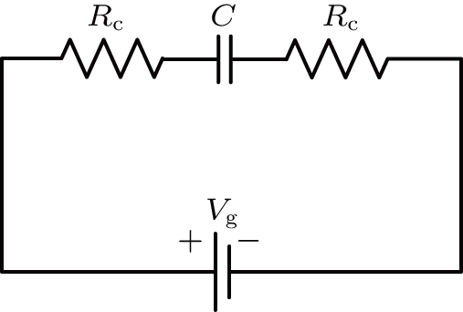
In the structure of Fig. 1, monolayer graphene sheet in the two semicircular holes and sandwiched silica served as dielectric spacer form a simple model of capacitance. The equivalent circuit[11,24] is shown in Fig. 2.

Fig. 2. The equivalent circuit of monolayer graphene electro-absorption modulator.

Based on the device structure in Fig. 2, the 3-dB bandwidth is estimated by

where R and C is the resistance and capacitance of the structure respectively. C is simple parallel plate capacitance, which could be calculated as C = ε0εrS/d, where S is overlap area of graphene sheet, d is the thickness of dielectric spacer.[12] And the equivalent resistance of the modulator is

where Rc is metal–graphene contact resistance. The values of contact resistance vary with different metal materials, suitably in our simulation Rc = 400 Ω⋅μm.[25] Lg = 1.47 μm is the metal–graphene contact length. As the chemical potential is proportional to the energy difference between the Femi level and the Dirac point, the critical driving voltage is defined as[13]

where VF = 3 × 10⁶ m/s is the Femi velocity, V0 is the voltage offset caused by natural doping, h is the reduced Planck constant, α = ε0εr/de is obtained from parallel-plate capacitor model of the used device.

The energy per bit refers to energy consumed by the modulator switch every time, which is depends on the capacitance C of the structure and voltage ΔV between on and off states of the modulator. The energy per bit is defined as

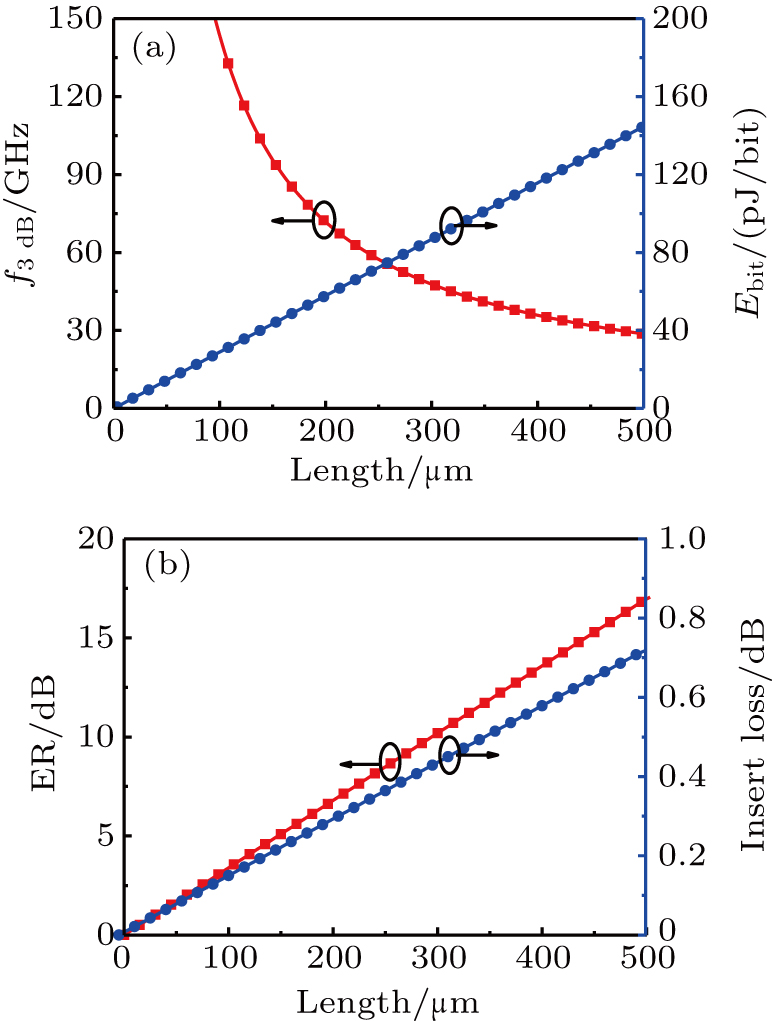
Based on the formulas above, the performances of modulator are shown in Figs. 3(a) and 3(b), 3-dB bandwidth decreases as the device length increases totally, but the extinction ratio, power consumption, and insertion loss all increase as the device length increases. For high-speed interconnection system, the extinction ratio should be larger than 7 dB, while for short-distance signal transmission, the extinction ratio should be larger than 4 dB. In summary, the extinction ratio (ER) for y-polarization mode can achieve 7 dB at 1550 nm by only using action region L = 205 μm, resulting in an energy per bit is 59 pJ/bit with insert loss of 0.29 dB. And the 3-dB bandwidth is estimated to be f3 dB = 70 GHz.

Fig. 3. (a) The 3-dB modulation bandwidth and energy per bit versus the length of active region, (b) extinction ratio and insert loss versus the length of active region.

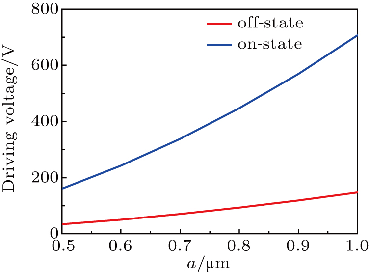
From the relationship between the external modulation voltage and the chemical potential of graphene in formula (3), the relationship between the modulation voltage at the switch point and the inner radius in the bend hole can be obtained. As the radius of silicon dioxide is in micron magnitude, modulator needs large voltage to change graphene’s chemical potential from 0.26 eV (off state) to 0.57 eV (on state), as shown in Fig. 4.

Fig. 4. Driving voltage of off state and on state versus inner radius.

Although the optimization of semicircular holes could reduce the voltage value, the silica in the fiber center is medium for light transmission, reducing its size will affect the transmission. Thereby, the size of the modulator selected is a = 0.66 μm, b = 1.9 μm, c = 0.6 μm, and larger voltage is needed to achieve the modulation effect, because the thickness of silicon dioxide is in the order of micron, its switch on and off voltages are 298 V and 62 V, respectively.

2.3. Principle of modulation

Due to the unique bandstructure of graphene, the interband absorption and intraband absorption should be considered, which can be evaluated from the Kubo formula[26] as follows:

where ω represents the angular frequency, μc is the chemical potential, Γ = 1/2τ is the scattering rate with τ as the relaxation time (τ1 = 10 fs is associated with intraband transitions, τ2 = 12 ps is associated with interband transitions). T is the temperature, e is the charge of the electrons, ħ is the reduced Planck constant, fd (E) is the Femi–Dirac distribution given by fd (E) = (e(Eμc)/kBT+1)−1, and kB is Boltzmam’s constant.

Then the graphene’s permittivity can be evaluated as

where ε0 is the vacuum permittivity, and the monolayer graphene thickness dg is 0.34 nm.

According to Maxwell’s equations, when spatial permeability μr ≈ 1, the relationship between permittivity and refractive index is as follows:

Based on the formula above, the permittivity ε and the refractive index n as a function of the chemical potential for the wavelength of λ = 1550 nm is sketched in Fig. 5.

Fig. 5. The graphene characters under different chemical potentials: (a) permittivity and (b) refractive index.

The real part of the permittivity Re(ε) firstly increases, then decreases with the chemical potential increasing. The imaginary part of the permittivity Im(ε) is almost constant from 0 eV to 0.3 eV, then decreases rapidly when the chemical potential is within the range of 0.3–0.5 eV. At the chemical potential μc = 0.5 eV, the Re(ε) changes from positive to negative (Fig. 5(a)). The real part of the refractive index Re(n) firstly increases, then decreases while the imaginary part of refractive index Im(n) changes in the opposite direction (Fig. 5(b)). Graphene is transformed from dielectric to metallic at μc = 0.5 eV, so 0.5 eV is called as epsilon-near-zero (ENZ) point. The change of permittivity will affect the change of effective refractive index and the imaginary part of the effective refractive index corresponds to the loss of light. Therefore, the intensity of the output light can be modulated by voltage control ultimately.

3. Simulation results and analysis
3.1. Characteristics of modulation

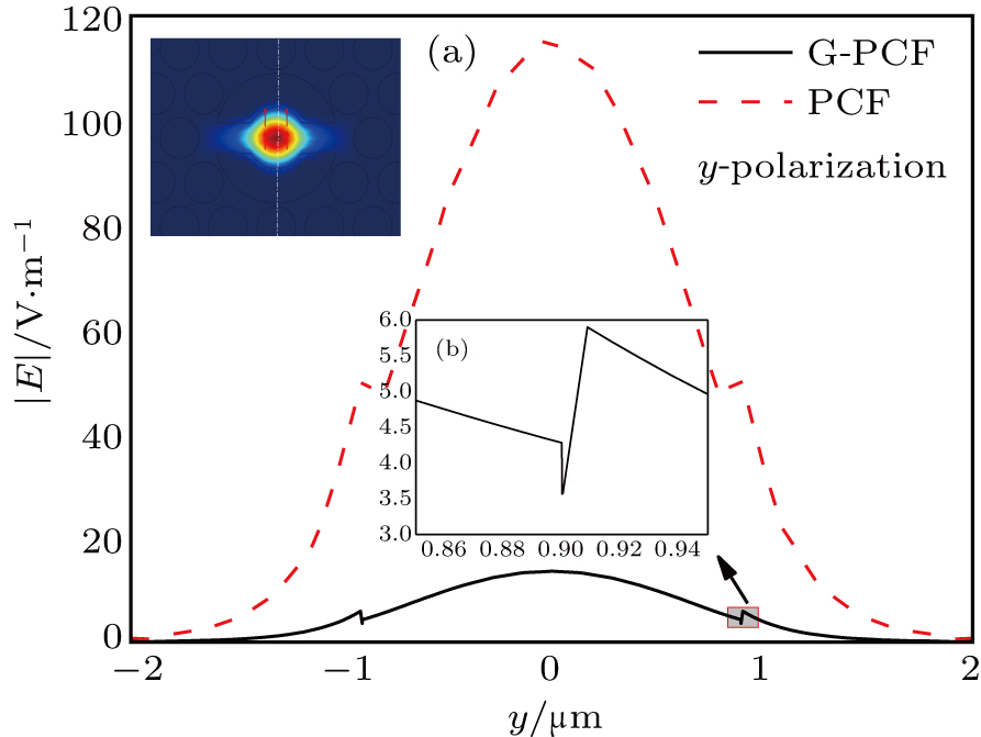
The mode field distribution of PCF after adding the graphene has been analyzed when the incident wavelength is 1550 nm. To evaluate the light absorption passed through the graphene film, the electric field distribution of y-polarization mode before and after graphene deposited along the y axis is analyzed as shown in Fig. 6.

Fig. 6. Electric field distribution of y-polarization mode with G-PCF and PCF.

In Fig. 6, the electric field in G-PCF is lower than that in PCF, given that the light is effectively coupled into the graphene, leading to the light attenuation. Due to the different refractive indexes, electric field has a jump in the graphene as shown in the inset of Fig. 6. Moreover, the real part Re(neff) and the imaginary part Im(neff) of effective refractive index for the G-PCF under different chemical potentials are displayed in Fig. 7.

Fig. 7. Re(neff) and Im(neff) of x-polarization and y-polarization modes under different chemical potentials.

In Fig. 7, we can see that Re(neff) continues its increasing trend from 0 eV to 0.4 eV, and reaches to its peak at 0.4 eV, then decreases and runs down to its minimum level at 1 eV. In addition, it is important to note that the real parts of effective refractive index of x-polarization and y-polarization modes make a great difference due to the asymmetry of structure. The variation trend of Im(neff) is similar to that of graphene’s permittivity versus the chemical potential. And the Im(neff) indicates the attenuation, which can be calculated by α = 8.686( 2π/λ)Im(neff). Thus, it proves that graphene’s permittivity affects the transmission of light in optical fiber. The transmission loss in different chemical potential is shown in Fig. 8.

Fig. 8. The corresponding loss versus chemical potential and the electric field profile (the inset of the figure).

In Fig. 8, it can be found that y-polarization mode produces a larger loss than x-polarization mode, which means y-polarization light can be more easily coupled. The insets in Fig. 8 show the mode field distribution of fundamental modes of x-polarization and y-polarization, respectively, and the arrows represent the direction of electric field. It must be emphasized that the loss of G-PCF varies largely near 0.4 eV. Chemical potential of 0.26 eV and 0.57 eV correspond to the maximum and minimum values with the losses of 18.23 dB/mm and 1.40 dB/mm respectively, namely ‘switch off’ state and ‘switch on’ state of optical switch. Therefore, it can be proved that graphene is qualified for the electro-absorption modulator due to its controllable Fermi energy by the applied voltage.

3.2. Influence factor of modulation
3.2.1. Chemical potential

The structural parameters of the optical fiber have great influence on the transmission of light field. Figure 9 shows the loss of G-PCF as functions of chemical potential under different inner radius of semicircular hole.

Fig. 9. Loss of G-PCF versus chemical potential for different semicircular hole’s inner radius.

In Fig. 9, it can be seen that different radius could not change the on–off position of the switch, but only change the difference between maximum and minimum loss Δα. In graphene, the ratio of light field energy to total energy of mode field is

When graphene is bound into an optical waveguide, the effective refractive index shows a linear relationship with the permittivity of graphene. fg determines the change of effective refractive index.[27] So the change of effective refractive index and permittivity of graphene with chemical potential is almost the same. fg changes near the ENZ point dramatically, which causes a small fluctuation in Im(neff). So there is a small peak around 0.5 eV in Fig. 9.

3.2.2. Semicircular hole’s inner radius and distance

As shown in Fig. 10, the difference between maximum and minimum loss Δα versus the inner radius a for the proposed G-PCF under different spacing of semicircular c.

Fig. 10. The loss difference of G-PCF versus inner radius for different semicircular hole’s distance.

In Fig. 10, it can be seen that the smaller value of a, the stronger interaction effect generated between graphene and light field. However, when a is small enough, Δα begins to decrease. This phenomenon is produced that most of the light is diffused into the cladding and not be limited to the core. In addition, the closer the two semicircular holes are, the more the light will be confined to the core, the greater Δα is. In principle, the greater Δα, the smaller the footprint of the modulator, the lower power consumption, the larger modulation bandwidth. Thus, the structure parameters of PCF is a = 0.66 μm, c = 0.6 μm, and Δα = 33.9 dB/mm.

3.2.3. Wavelength

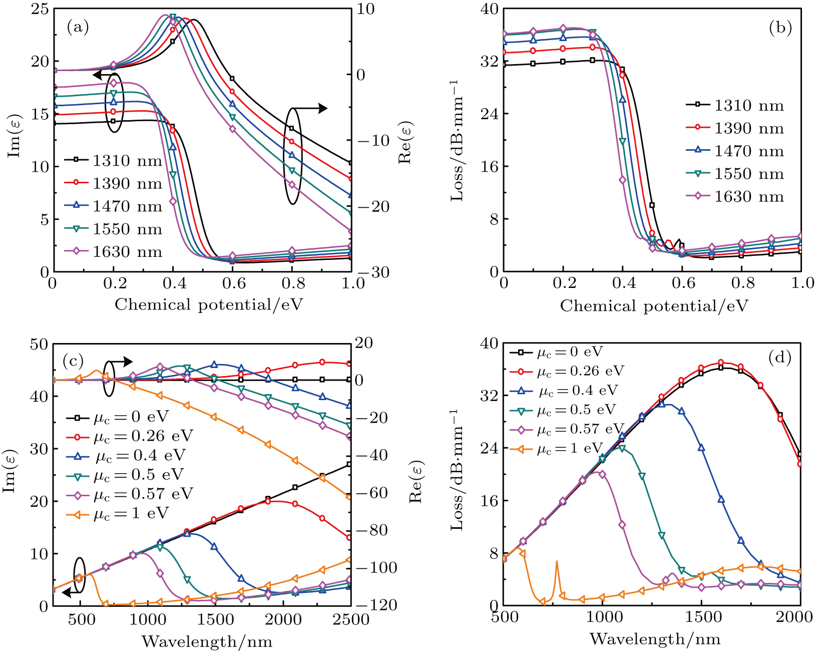
Previous studies have been performed the permittivity also varies with the different wavelengths at 1550 nm, since graphene’s conductivity is related to the optical wavelength as shown in Fig. 11.

Fig. 11. (a) The permittivity of graphene as a function of chemical potential at wavelengths of 1310, 1390, 1470, 1550, and 1630 nm, and (b) the corresponding losses. (c) The permittivity of graphene as a function of wavelength at chemical potentials of 0, 0.26, 0.4, 0.5, 0.57, and 1 eV, and (d) the corresponding losses.

As shown in Figs. 11(a) and 11(b), the permittivity and the loss of G-PCF are influenced by the wavelength strongly. As the wavelength increases, the peak of the real part of the permittivity moves to the lower chemical potential, and also corresponds to the overall moving direction of the imaginary part. In Fig. 11(b), the trends of loss and imaginary part are approximately similar, because the imaginary part reflects the variation of loss. The “on–off” points are 0.6 eV and 0.31 eV under the 1310 nm. With the wavelength increasing, the point of the modulator decreases to 0.51 eV and 0.25 eV at 1630 nm. Therefore, the “on–off” points can be changed by changing the incident light frequency.

To evaluate the operating wavelength of the modulator, the wavelength was studied at different chemical potentials in Figs. 11(c) and 11(d). For μc = 1 eV, the dispersion spectrum of Re(ε) firstly increases and reaches to its high value at λ = 620 nm, which is the intraband transition threshold according to μc = hc/2λ. Simultaneously, this point corresponds to the the largest inclined rate of Im(ε). Then Re(ε) decreases after λ > 620 nm since intraband transitions play the dominant role. At λ = 780 nm, it changes from positive value to negative value, which is called ENZ point. With the decreasing of chemical potential, transition threshold point occurs to red shift, and Im(ε) follows with it. The loss spectra of G-PCF (Fig. 11(d)) is almost identical to that of Im(ε). It shows two characteristic features: the position of the loss peak corresponds to the imaginary part of the permittivity peak, and the secondary loss peak coincides with ENZ point. With chemical potential shifts to lower energy, the loss peak and the secondary peak move to long wavelength, and the loss peak becomes larger, the bandwidth becomes wider, and the secondary peak decreases gradually. The cause of these changes is that loss peak is mainly caused by the electron interband transition of graphene, and the secondary peak is caused by intraband transition. When the light incident occurs, the electron at the Fermi energy could take an interband transition with the satisfaction of μc = hc/2λ, but when the Fermi energy is lower than half of the photon energy, the interband transition will be suppressed, and the intraband transition will increase. The maximum loss difference is observed around 1550 nm. The operating wavelength (full width half bandwidth) ranging from 1250 nm to 1900 nm that results in optical wavelength longer than 650 nm centered around 1550 nm.

4. Conclusion

In summary, we have proposed a compact electro-absorption modulator based on graphene photonic crystal fiber. The performance of the device is investigated by theoretical simulation on the basis of the controllable electric properties of graphene Fermi level. Simulation results shows that the electric field distribution decreases sharply in G-PCF in terms of electrons absorption by graphene, and switch on–off point of modulator is only related to the frequency of incident light. Geometric parameters of PCF could significantly change the effective mode index of fundamental mode and losses. By optimizing these parameters, the electro-absorption modulator can achieve some good characters including an extinction ratio 7 dB of y-polarization mode, 3-dB modulation bandwidth of 70 GHz with small footprint of 205 μm, and a consumption of energy per bit 59 pJ/bit. This modulator can work over a wide wavelength range from 1250 nm to 1900 nm.

Reference
[1] LiuZ B FengM JiangW S XinW WangP ShengQ W LiuY G WangD N ZhouW Y TianJ G 2013 Laser Phys. Lett. 10 065901
[2] García-GrandaM HuH Rodríguez-GarcíaJ SohlerW 2009 J. Lightw. Technol. 27 5690
[3] NovoselovK S GeimA K MorozovS V 2004 Science 306 666
[4] PallecchiE LafontL CavaliereV 2015 Sci. Rep. 4 4558
[5] NairR R BlakeP GrigorenkoA N 2008 Science 320 1308
[6] StauberT PeresN M R GeimA K 2008 Phys. Rev. 78 085432
[7] WangF ZhangY B TianC S 2008 Science 320 206
[8] LiZ Q HenriksenE A JiangZ MartinM C KimP StormerH L BasovD N 2008 Nat. Phys. 4 532
[9] LiuM YinX B Ulin-AvilaE GengB S Zent grafT JuT WangF ZhangF 2011 Nature 474 64
[10] GosciniakJ TanD T H 2013 Nanotechnology 24 185202
[11] YeS W WangZ S TangL F 2014 Opt. Express 22 26173
[12] ZhuH Y LiuM J 2000 J. Neijiang Normal University 15 18 in Chinese
[13] ZhouF JinX F HaoR ZhangX M ChiH ZhengS L 2016 J. Opt. 45 1
[14] ShahM K YeS W ZouX H YuanF JhaA ZhangY L LuR G LiuY 2016 IEEE J. Sel. Top. Quantum Electron. 23 1
[15] DashJ N JhaR 2014 IEEE Photon. Technol. Lett. 26 595
[16] ZouH XiongH ZhangY S MzY ZhengJ J 2017 Chin. Phys. 26 124216
[17] ZhaoJ Q RuanS C YanP G ZhangH YuY Q WeiH F LuoJ 2013 Opt. Eng. 52 106105
[18] SinghS PrajapatiY K 2019 Appl. Phys. 125 437
[19] SunJ Y ChenY B PriydarshiM K ChenZ BachmatickA ZouZ Y ChenZ L SongX J GaoY F RümmeliM H ZhangY F LiuZ F 2015 Nano Lett. 15 5846
[20] SunJ LindvallN ColeM T WangT BoothT J 2012 Appl. Phys. 111 044103
[21] FangH MaR L WeiH F 2012 J. Xi’an Technol. University 32 187 in Chinese
[22] LiH F 2015Research on Fiber Transmission Characteristics of Photonic Crystal and Splice LossMS DissertationChangchunChangchun University of Science and Technologyin Chinese CNKI:CDMD:2.1015.997128
[23] TongL M LouJ Y MazurE 2004 Opt. Express 12 1025
[24] BiW H WangY Y FuG W WangX Y LiC L 2016 Acta Phys. Sin. 65 047801 in Chinese
[25] KoesterS J LiM 2012 Appl. Phys. Lett. 100 171107
[26] HansonG W 2008 J. Appl. Phys. 103 064302
[27] HaoR DuW ChenH S JinX F YangL Z LiE P 2013 Appl. Phys. Lett. 103 061116