|
Chen Qiao-Yue1, Song Jun-Jie3, Jing Liwei1, Huang Kaikai1, He Pimo1, 2, ‡, Zhang Hanjie1, †
|
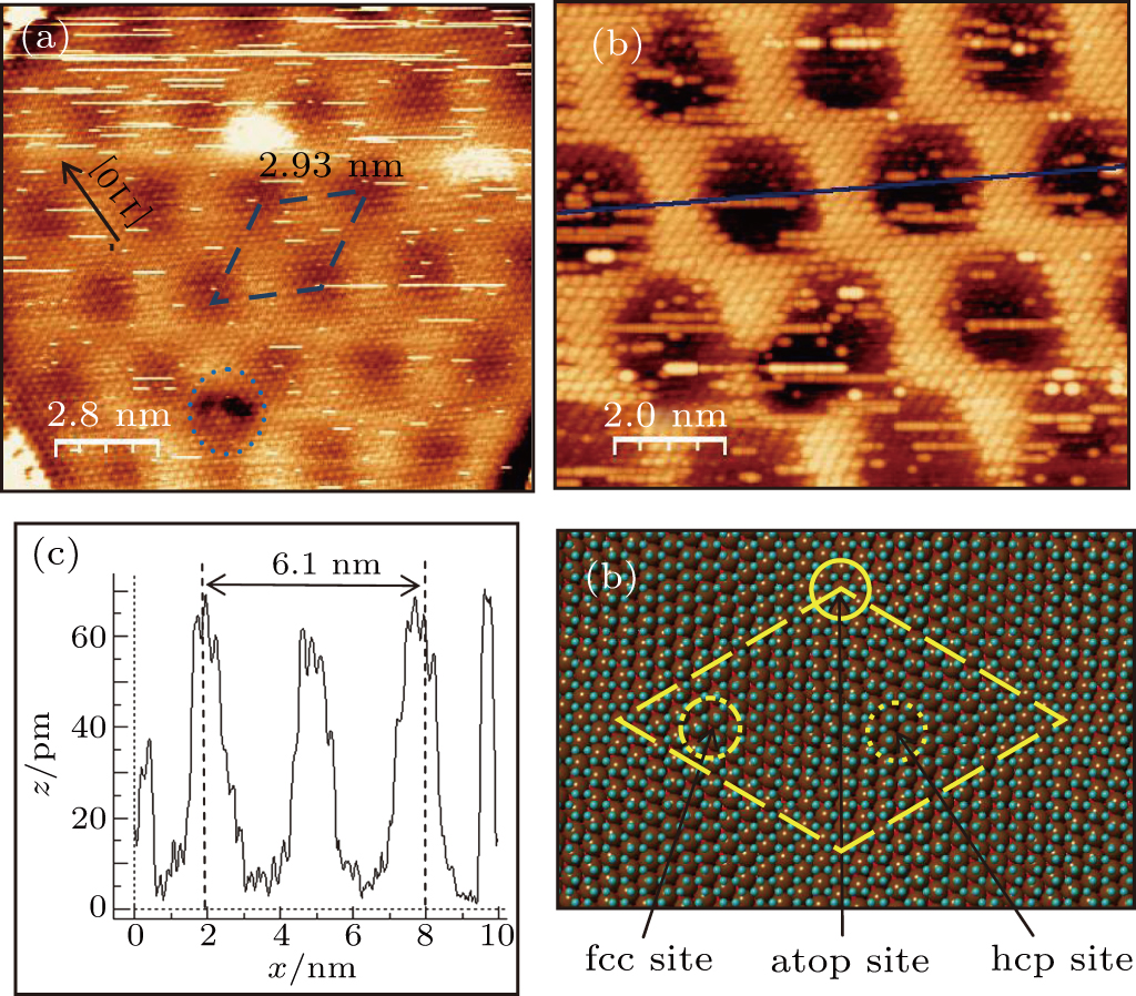
(a) STM topography of superstructure of graphene on Cu (111) with a periodicity of 2.93 nm (14 nm × 14 nm, VT = −0.172 V, IT = 0.558 nA), and the black arrow indicates the [110] direction of Cu(111). (b) High resolution STM topography (10 nm × 10 nm, VT = −0.183 V, IT = 0.403 nA). (c) Line profile along the blue straight line outlined in Fig. 3(b). (d) Simulation result through simply align graphene to Cu(111) with 4° rotation and the superscell is (
133×133
)R4.3°, as outlined with yellow rhombus. The blue balls represent carbons and brown, red, black balls represent the first, second, third layer copper atoms. The fcc, hcp, and atop adsorption sites have been marked with yellow circles to describe the location of carbon rings on Cu(111). |
