


Analysis of highly efficient perovskite solar cells with inorganic hole transport material
Cite this Article
Kabir I, Mahmood S A. Analysis of highly efficient perovskite solar cells with inorganic hole transport material. Chinese Physics B, 2019, 28(12): 128801 
Permissions
Analysis of highly efficient perovskite solar cells with inorganic hole transport material
† Corresponding author. E-mail:
Abstract
Organo-halide perovskites in planar heterojunction architecture have shown considerable promise as efficient light harvesters in solar cells. We carry out a numerical modeling of a planar lead based perovskite solar cell (PSC) with Cu2ZnSnS4 (CZTS) as the hole transporting material (HTM) using the one-dimensional solar cell capacitance simulator (SCAPS-1D). The effects of numerous parameters such as defect density, thickness, and doping density of the absorber layer on the device performance are investigated. The doping densities and electron affinities of the electron transporting material (ETM) and the HTM are also varied to optimize the PSC performance. It has been observed that a thinner absorber layer of ∼220 nm with a defect density of 1014 cm−3 compared to the reference structure improves the device performance. When doping density of the absorber layer increases beyond 2 × 1016 cm−3, the power conversion efficiency (PCE) reduces due to enhanced recombination rate. The defect density at the absorber/ETM interface reduces the PCE as well. Considering a series resistance of 5 Ω · cm2 and all the optimum parameters of absorber, ETM and HTM layers simultaneously, the overall PCE of the device increases significantly. In comparison with the reference structure, the PCE of the optimized device has been increased from 12.76% to 22.7%, and hence the optimized CZTS based PSC is highly efficient.
1. Introduction
The rate of energy consumption increases to cope with economic development. However the source of nonrenewable energy decreases gradually. Among other renewable energy sources, solar cells have drawn a great deal of attention from researchers. Over the past decade, many studies have been carried out on organo-halide perovskite solar cells (PSCs).[1–4] In comparison with traditional solar cells, they have simpler processing techniques, higher power conversion efficiency (PCE), and lower cost.[5] In 2009, Miyasaka et al. first introduced the PSCs using MAPbI3 (MA = CH3NH3) and MAPbBr3 as light harvesters although their PCEs are low (3%–4%).[6] Recently, the PCEs of lead based PSCs have reached ∼22.1%.[1,7] The PCEs have reached above 25% when PSC is used in silicon based tandem solar cells.[8] The absorption coefficient of MAPbX3 is very high (103–104 cm−1) along with high charge carrier mobility (2–66 cm2 · V−1 · s−1).[7] The tunable band gap (1.55–2.50 eV) property of this material can be utilized to make colorful solar designs.[9] In addition, MAPbX3 based thin films have charge carrier life time of ∼270 ns and carrier diffusion length of 100–1900 nm.[7]
The planar PSC structure, where a thin perovskite layer is sandwiched between layers of a hole transporting material (HTM) and an electron-transporting material (ETM), is preferred due to simple fabrication technique.[10] According to the order of preparation, the planar PSC structure can be either n–i–p or p–i–n. Organic compounds, such as spiro-MeOTAD, PEDOT:PSS, PTAA and P3HT are the commonly used HTMs in the case of high-efficient PSCs.[2,11–13] However, most of the organic based HTMs are unstable and costly. The reduction in PCE of spiro-MeOTAD based PSC is more than 50% after 15 days under moisture and heat.[14] The complex and time consuming synthetic process make the spiro-MeOTAD based PSCs costly as well.[2] PEDOT:PSS is chemically unstable due to its acidic and hygroscopic nature.[15] The contraction of PEDOT conductive grains leads to the thermal instability of PEDOT:PSS films.[15] The PCE of PEDOT:PSS based PSC reduces by 40% within 10 days.[16] The highest PCE achieved by PTAA based PSC is 21.2% and the PCE degradation is ∼5% in 20 days.[11,17] The PCE of pristine P3HT based PSC is only 14.3% and degraded by 20% within 29 days.[18]
Inorganic HTMs are preferable as they are cheaper, more stable, and simple to synthesize. Recently, Cu based HTMs such as CuI, CuSCN, Cu2O, CuInGaSSe, and Cu2ZnSnS4 (CZTS) draw attention of researchers.[19–23] The reported PCE of CuI based PSC is 17.6% and the PCE decreases by 8% within 90 days.[22] Although its stability is comparable to PTAA based PSC, the PCE is lower than the organic counterpart. Its mesoporous structure increases the process complexity and hence industrially less preferable.[24] The PCE of CuSCN based inverted planar PSC is 15.6% and degraded by 20% within 2 days.[19] A PCE of 13.35% is achieved by Cu2O based inverted planar PSC and sustained above 90% of initial value for 70 days.[20] Another mesostructured PSC with CuInGaSSe as HTM achieves a PCE of 9.15% and sustained 90% of initial value for 5 days. Kesterite materials, e.g., CZTS, are an efficient light harvester for thin film solar cells due to their high absorption coefficient (∼104 cm−1), optimal band gap (1.4–1.5 eV) for solar energy conversion, high hole mobility (6–35 cm2·V−1 · s−1), and earth abundant constituents.[25] However, the highest PCE of CZTSSe based thin film solar cell is 12.6%.[21] Wu et al. have shown that Cu2ZnSnS4 (CZTS) can be used as a nontoxic and low cost HTM in planar lead based PSC.[25] It increases the light absorbance of the device and hence increases the short circuit current density of the PSC. Surface recombination can also be reduced by using CZTS layer as an HTM in PSCs.[25] Zuo et al. have employed CZTS nanoparticle as an HTM in lead based planar PSC and achieved a PCE of 13.41%.[26] They have also demonstrated an improved crystallinity of the perovskite film. In another work it has been exhibited that CZTS based PSC sustains more than 98% of its initial PCE for 3 days.[21] For ETM, TiO2 is the most widely used materials both in planar and mesostructured PSC.[27] Currently the PCE of planar PSCs is lower than the mesostructured devices.[28] Apart from experimental works, a theoretical investigation is necessary to improve the performance of the planar PSC. Many researchers have used one dimensional solar cell capacitance simulator (SCAPS-1D) to simulate the PSC and other thin film solar cells.[29]
Recently, Kabir et al. have analyzed the MAPbI3 based PSC with CZTS as the HTM, and optimized a few parameters such as absorber layer thickness and doping density of different layers to improve the PCE of the device.[30] In this paper, the defect density, doping concentration, and thickness of the absorber layer are varied to optimize the device performance. The effects of doping concentration and the electron affinity of the HTM and the ETM on the device performance have been investigated. The hole mobility of the HTM and the defect density at the ETM/absorber and absorber/HTM interfaces are also varied to improve the PCE of the device. This work will be very helpful to design a highly efficient lead based planar PSC with CZTS as the HTM.
2. Simulation Method and Device Model
Many researchers used the SCAPS-1D solar cell simulator to analyze the device performances such as quantum efficiency (QE), energy band diagram, J–V curve, fill factor (FF), power conversion efficiency (PCE), short circuit current density Jsc and open circuit voltage Voc. Figure
 | Fig. 1. Structure of an n–i–p planar PSC. |
Table
Figure
 | Fig. 2. Absorption coefficients of different materials. |
| Table 1. The material parameters of different layers considered in the simulation. . |
3. Results and discussion
3.1. Model validation
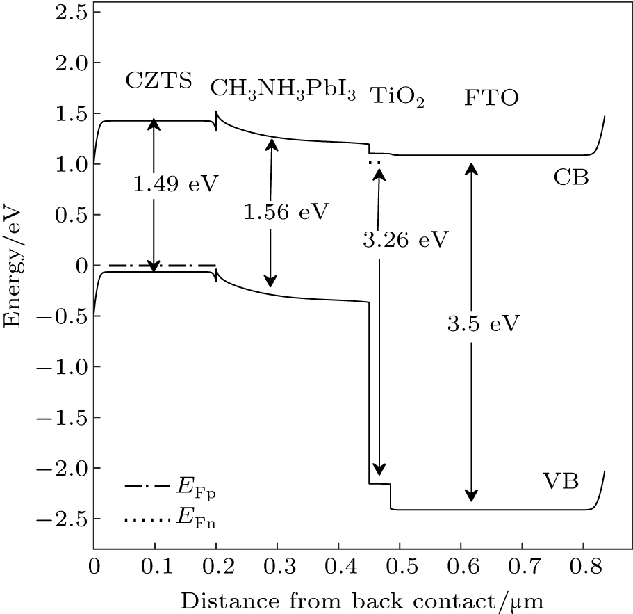
Figure
 | Fig. 3. Simulated energy band diagram of the device. |
3.2. Effect of the defect density of the absorber on the PSC performance
The defect density of the absorber layer has a significant impact on the device performance. Absorber with larger grain size has lower defect density, longer diffusion length, and higher charge carrier mobility.[40] Figure
 | Fig. 4. Effect of defect density of absorber layer on the device performance. |
| Table 2. Variations of the charge carrier diffusion length with the defect density of absorber layer. . |
3.3. Effect of the thickness of the absorber layer
The thickness of the absorber layer affects the device performance. Optimum absorber thickness ensures an efficient charge collection by balancing both absorption and recombination altogether in the device.[42] Figure
 | Fig. 5. Effect of the thickness of absorber layer on the device performance. |
3.4. Effect of electron affinities of ETM and HTM
The band offset of the PSC structure plays an important role in determining charge carrier recombination at the interfaces.[44] It also quantifies the Voc of the PSC. The band offsets can be tailored by changing the electron affinities of ETM and HTM. Figure
 | Fig. 6. Effect of electron affinity of ETM on the device performance. |
Figure
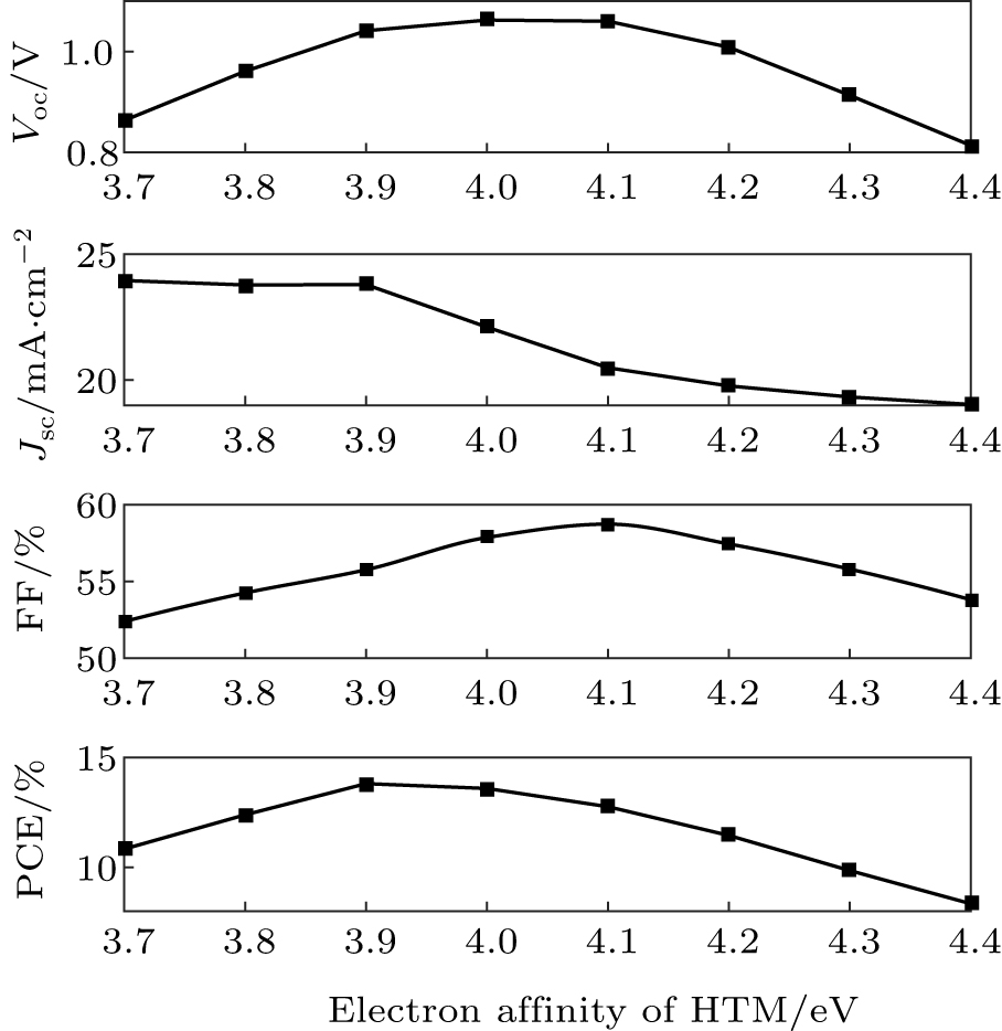 | Fig. 7. Effect of electron affinity of the HTM on the device performance. |
3.5. Effect of the defect density at the interface
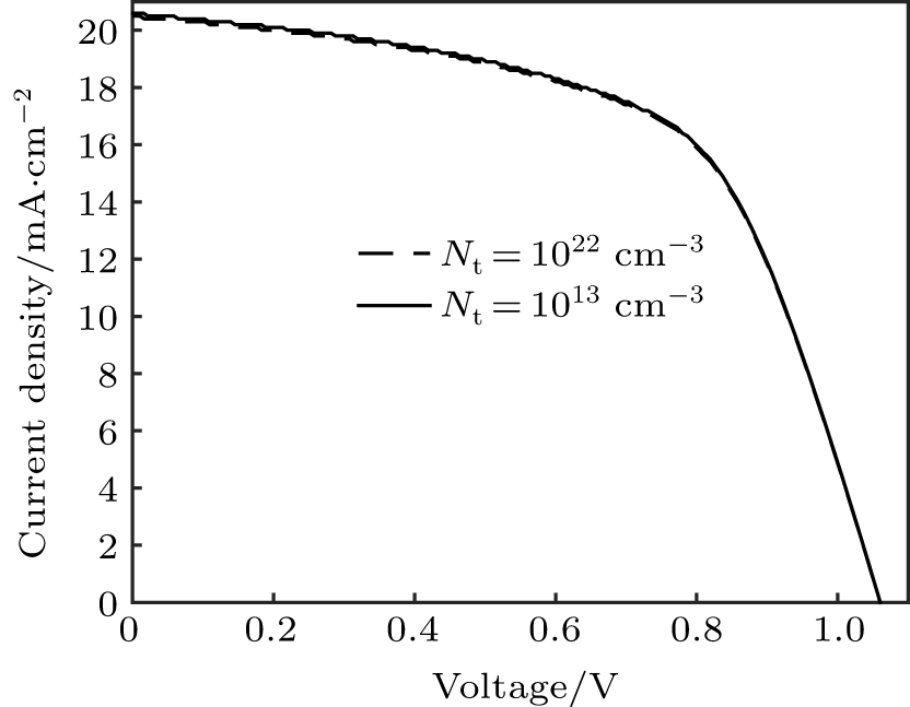
The interface quality at the heterojunction affects the device performance. Specially, interface defect density at the absorber/ETM and absorber/HTM has a significant effect on the device performance.[31,32] Figure
 | Fig. 8. J–V characteristics of PSC for various defect densities of IL2. |
 | Fig. 9. J–V characteristics of PSC for various defect densities of IL1. |
3.6. Effect of doping densities of absorber, ETM, and HTM
Doping plays a vital role to improve the performance of the halide based PSC. As doping density increases, charge carrier concentrations also increases. However, ionized impurity introduces scattering centers in the crystal structure which reduces the charge carrier mobility. Moreover, deep traps are generated due to high doping density.[45] Figure
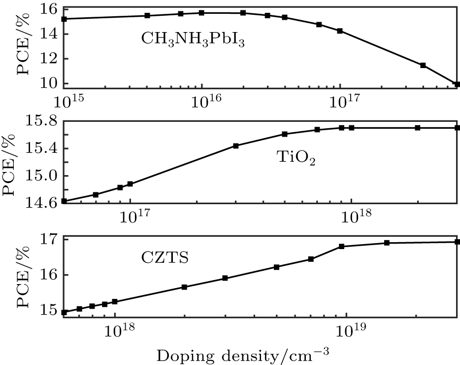 | Fig. 10. The PCE of the PSC for various doping densities of the absorber, ETM, and HTM. |
3.7. Determination of the optimized PSC structure
Table
 | Fig. 11. J–V characteristics of the PSC. The dotted line and the solid line represent the simulated results considering the reference parameters and the optimum parameters, respectively. |
| Table 3. Optimum parameters of the device. . |
| Table 4. Comparison of the performance between the reference structure parameters and the optimum parameters. . |
As mentioned above, CZTS has also been used as an active layer in thin film solar cells. The best reported PCE of CZTS based thin film solar cell is 11%.[48] Various synthesis techniques have been used to improve the PCE of CZTS based photovoltaic devices. The complex synthesis process forms secondary phases which degrades the CZTS film quality and hence limits the solar cell efficiency.[49]
4. Conclusion
A lead based PSC with CZTS as inorganic HTM has been analyzed by SCAPS-1D device simulator. Consistent material parameters are taken from the literature. The relative permittivity, electron affinity, band gap, and charge carrier mobility of the absorber layer are the same as those in the reference structure. For the ETM and the HTM, the thickness, relative permittivity, band gap, and defect density are also the same as those in the reference structure. The simulated result illustrates that the performance of the reference PSC can be improved taking an optimum absorber layer defect density of ∼ 5 × 1014 cm−3. The optimum thickness of absorber layer (∼ 220 nm) has been found, which increases the PCE. The doping in the absorber layer has also been optimized to increase the PCE from 12.76% to 15.69%. It has been observed that a doping density beyond 2 × 1016 cm−3 in the absorber layer reduces the PCE of the device due to enhanced recombination rate. Electron affinities of 3.9 eV and 3.85 eV for the HTM and the ETM, respectively are found to increase the PCE of the reference PSC from 12.76% to 15.57%. It has also been found that the defect density at the absorber/HTM interface has negligible effect on the device performance. The defect density at the absorber/ETM interface has significant effect on the device performance as most of the carrier generated near this interface. The overall PCE of the reference PSC increases from 12.76% to 22.7% by considering a series resistance of 5 Ω·cm2, and the optimum parameters of absorber, ETM and HTM layers simultaneously. The PCE of the optimized PSC has been increased significantly compared to the reference structure. Hence, the optimized PSC structure with CZTS as the HTM is highly efficient.
Reference
| [1] | |
| [2] | |
| [3] | |
| [4] | |
| [5] | |
| [6] | |
| [7] | |
| [8] | |
| [9] | |
| [10] | |
| [11] | |
| [12] | |
| [13] | |
| [14] | |
| [15] | |
| [16] | |
| [17] | |
| [18] | |
| [19] | |
| [20] | |
| [21] | |
| [22] | |
| [23] | |
| [24] | |
| [25] | |
| [26] | |
| [27] | |
| [28] | |
| [29] | |
| [30] | |
| [31] | |
| [32] | |
| [33] | |
| [34] | |
| [35] | |
| [36] | |
| [37] | |
| [38] | |
| [39] | |
| [40] | |
| [41] | |
| [42] | |
| [43] | |
| [44] | |
| [45] | |
| [46] | |
| [47] | |
| [48] | |
| [49] |