


Simulation of a-Si:H/c-Si heterojunction solar cells: From planar junction to local junction
Cite this Article
Huang Haibin, Zhou Lang, Yuan Jiren, Quan Zhijue. Simulation of a-Si:H/c-Si heterojunction solar cells: From planar junction to local junction. Chinese Physics B, 2019, 28(12): 128503 
Permissions
Simulation of a-Si:H/c-Si heterojunction solar cells: From planar junction to local junction
† Corresponding author. E-mail:
Project supported by the National Key R&D Program of China (Grant No. 2018YFB1500403), the National Natural Science Foundation of China (Grant Nos. 11964018, 61741404, and 61464007), and the Natural Science Foundation of Jiangxi Province of China (Grant No. 20181BAB202027).
Abstract
In order to obtain higher conversion efficiency and to reduce production cost for hydrogenated amorphous silicon/crystalline silicon (a-Si:H/c-Si) based heterojunction solar cells, an a-Si:H/c-Si heterojunction with localized p–n structure (HACL) is designed. A numerical simulation is performed with the ATLAS program. The effect of the a-Si:H layer on the performance of the HIT (heterojunction with intrinsic thin film) solar cell is investigated. The performance improvement mechanism for the HACL cell is explored. The potential performance of the HACL solar cell is compared with those of the HIT and HACD (heterojunction of amorphous silicon and crystalline silicon with diffused junction) solar cells. The simulated results indicate that the a-Si:H layer can bring about much absorption loss. The conversion efficiency and the short-circuit current density of the HACL cell can reach 28.18% and 43.06 mA/cm2, respectively, and are higher than those of the HIT and HACD solar cells. The great improvement are attributed to (1) decrease of optical absorption loss of a-Si:H and (2) decrease of photocarrier recombination for the HACL cell. The double-side local junction is very suitable for the bifacial solar cells. For an HACL cell with n-type or p-type c-Si base, all n-type or p-type c-Si passivating layers are feasible for convenience of the double-side diffusion process. Moreover, the HACL structure can reduce the consumption of rare materials since the transparent conductive oxide (TCO) can be free in this structure. It is concluded that the HACL solar cell is a promising structure for high efficiency and low cost.
1. Introduction
In the past few decades, hydrogenated amorphous silicon/crystalline silicon (a-Si:H/c-Si) based heterojunction solar cells have been attractive since they possess high open-circuit voltage (Voc), low-cost fabrication process and low temperature coefficient.[1–10] In 1992, Panasonic company developed an a-Si:H/c-Si heterojunction structure called the HIT (heterojunction with intrinsic thin-layer) solar cell.[1] Up to now, the conversion efficiency of the typical HIT solar cell has reached 24.7%.[4] For the HIT solar cell, the doped a-Si:H layer at the illumined front of the cell acts as the emitter, and the intrinsic a-Si:H layer plays a role of passivating defects. However, the a-Si:H material can bring about large optical absorption because it possesses a very high absorption coefficient. Holman et al.[11] showed theoretically that a relative efficiency increase of over 5% is possible for the heterojunction solar cell by mitigating parasitic absorption. In order to minimize the absorption loss of the a-Si:H, some researchers attempted to develop high-quality wide-gap alloys, such as a-SiC:H,[12] a-SiOx:H,[13] μc-SiOx:H[14] and μc-3C-SiC,[15] to replace a-Si:H as an emitter of the heterojunction solar cell. However, so far, the performance improvement of the solar cell is limited. The reason may be that the property of alternative materials is not good enough and big band offset deteriorates cell performance.[12,16] Several groups[17–21] reported that the emitter of the a-Si:H layer can be placed at the back side of the cell for avoiding the absorption of the doped a-Si:H layer, i.e., interdigitated back contact (IBC) technology has been used for the silicon heterojunction solar cell. The solar cell with the combination of the HIT and IBC technologies has achieved a world-record efficiency of over 26%.[20,21] However, the structure with the HIT and IBC technologies is very complicated, and it is not convenient to fabricate for mass production. In our previous work,[22] we employed an n-type c-Si layer as the emitter, in other words, the doped and intrinsic a-Si:H layers are replaced by n-type c-Si for reducing the optical absorption loss. This device is called the HACD (heterojunction of amorphous silicon and crystalline silicon with diffused junction) cell. However, the c-Si emitter in this structure, which is heavy doped, can make more recombination since the surface of the silicon wafer is also the region where the photocarriers are most generated. In order to overcome the above issues, we propose a bifacial heterojunction of amorphous/crystalline silicon with localized p–n structure (HACL cell).[23,24] The HACL cell structure can minimize the absorption loss of the a-Si:H and reduce recombination of photocarriers in the emitter. All of p–n junctions are local for the HACL cell. The local p–n-junction can make the cell keep high open-circuit voltage, and also take full advantage of sunlight and reduce photocarrier recombination. In addition, the TCO layer, in which it contains rare and expensive indium, can be free for the HACL cell so that the cost will be reduced.
In this work, we perform a numerical simulation using the ATLAS program.[25] The effect of the doped a-Si:H layer on the performance of the HIT cell is studied. The structure of the HACL solar cell is designed. The performance improvement mechanism for the HACL cell is explored. The potential performances of the HIT, HACD and HACL cells are evaluated. The HACL cell with single-side planar junction and single-side local junction are analyzed. All n-type or p-type c-Si passivating layers for the HACL cells are discussed.
2. Device model and simulation parameters
where ψ is the electrostatic potential, ε is the local permittivity, and ρ is the local space charge density. Here ρ is the sum of contribution from all mobile and fixed charges, including electrons, holes and ionized impurities.
where n and p are the electron and hole concentrations, J n and J p are the electron and hole current densities, Gn and Gp are the generation rates for electrons and holes, Rn and Rp are the recombination rates for electrons and holes, and q is the magnitude of the charge on an electron.
where GAO(E) and GDO(E) are the states per volume per energy for tail states at EV and EC, and EA and ED are the characteristic energies that determine the slopes of their respective tails.
where NAG and NDG are the states per volume per energy for acceptors and donors, EAK and EDK are the peak energy position of Gaussian, and σA and σD are the standard deviation of Gaussian acceptors and donors.
Figure
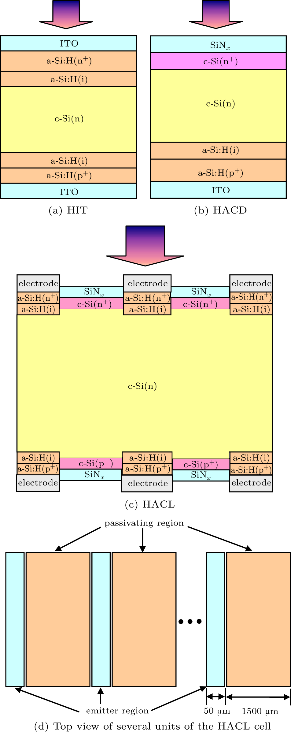 | Fig. 1. Schematic of silicon heterojunction solar cells with different structures: (a) HIT, (b) HACD, (c) HACL, and (d) top view of several units of the HACL cell. |
The ATLAS program is used in this study. The simulation method is based on the Poisson equation, and the electron and hole continuity equations,[25]
 |
 |
 |
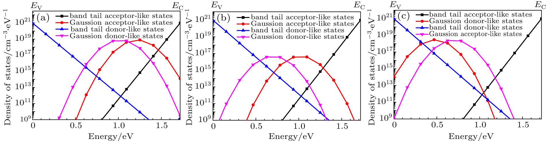
For an a-Si:H material, the density of states in the bandgap is assumed to be both acceptor-like states and donor-like states modeled by Gaussian mid-gap states (associated with silicon dangling bonds) and exponential band tails. The conduction and valence band tail states can be described as follows:
 |
 |
The Gaussian mid-gap states of acceptor-like states and donor-like states are given by
 |
 |
The band tail states and Gaussian mid-gap states of doped and intrinsic a-Si:H layers are shown in Fig.
 | Fig. 2. Gap defect state distribution of (a) a-Si:H(p+), (b) a-Si:H(i), and (c) a-Si:H(n+) layer. |
The main material parameters[22,26,27] used in this simulation are listed in Table
| Table 1. Main parameters used for the simulation of HIT, HACD and HACL solar cells. . |
3. Results and discussion
3.1. Effect of the doped a-Si:H layer on the performance of the HIT cells
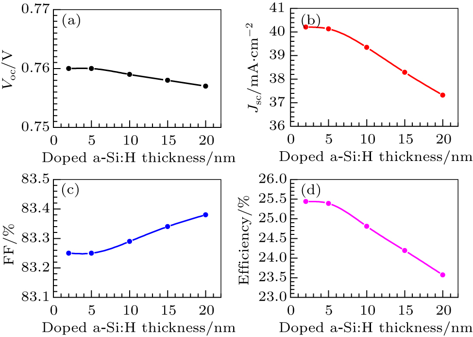
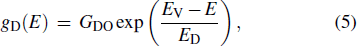
For an HIT solar cell, the planar junctions are assembled at top and bottom sides of the device. The emitter of the a-Si:H layer entirely covers the surface of the c-Si base. The large absorption coefficient of the a-Si:H material can bring about absorption losses. In order to assess the loss, the performance of the HIT cell is calculated in dependence of variable thicknesses of the top doped a-Si:H layer. Figure
 | Fig. 3. Photovoltaic parameters of the HIT cells with the emitters of different thicknesses. |
 | Fig. 4. IQE curves of the HIT cells with the emitters of different thicknesses. |
3.2. Performance improvement mechanism for HACL cells
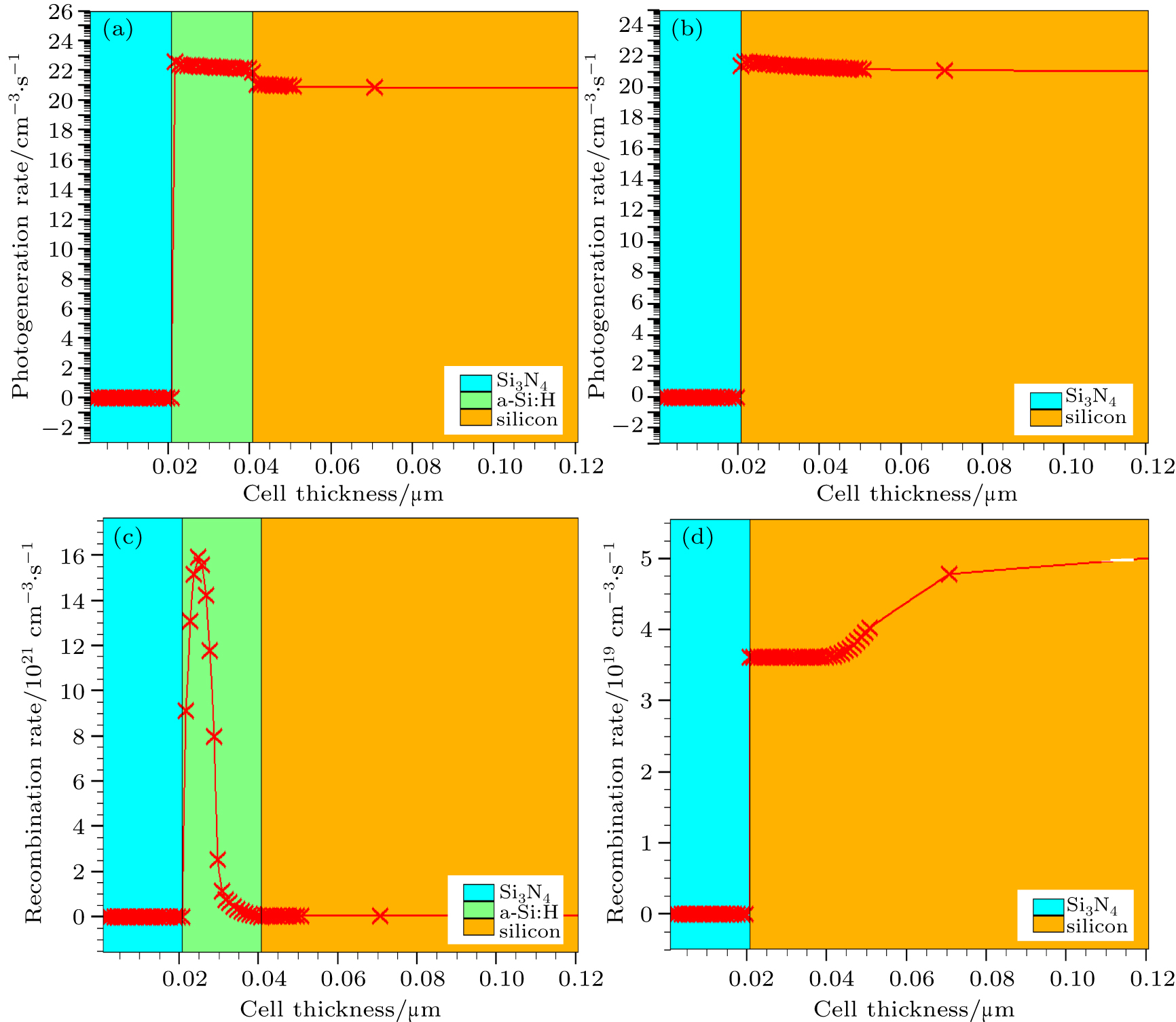
In order to minimize the absorption loss of a-Si:H, the local p–n junctions are designed for the HACL cells. The photogeneration rate and the recombination rate are calculated as shown in Fig.
 | Fig. 5. The photogeneration rate and the recombination rate of different regions for the HACL cell: (a) and (c) for the region that is perpendicular to the emitter region surface, (b) and (d) for the region that is perpendicular to the passivating region surface. |
Compared to the HACD cell, the HACL structure can reduce the photocarrier recombination in the emitter. For the HACL cell, most of the surface area is covered by the c-Si passivating layer. The c-Si passivating layer is very thin (about dozens of nanometers), so the recombination quantity is little. Moreover, the recombination rate in the c-Si passivating layer is not large. We can see from Fig.
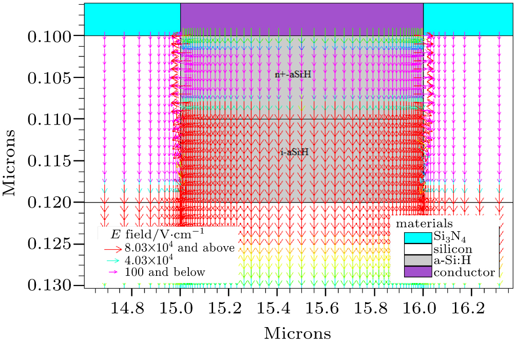
For the HACL cell, its structure can help photocarriers to be better transported and collected. In order to illustrate the argument, the vector of electric field for the top side of the part HACL cell is plotted as shown in Fig.
 | Fig. 6. Vector of electric field for the top side of the part HACL cell. |
To verify the advantage of the HACL structure, potential performances of the HIT, HACD and HACL cells are calculated. Figure
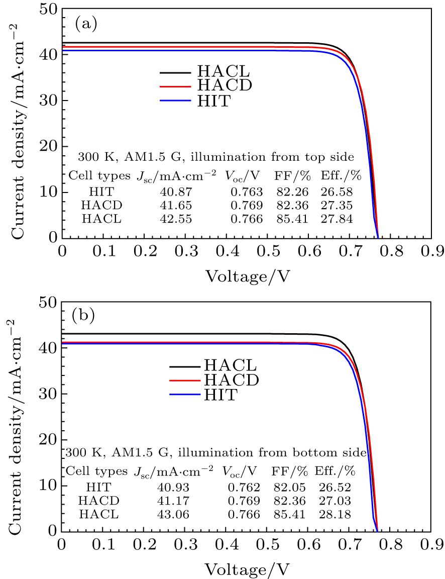 | Fig. 7. Potential performances of the HIT, HACD and HACL cells: (a) illumination from top side, (b) illumination from bottom side. |
Here it should be noted that in our previous work[22] a conversion efficiency of 28.55% can be achieved for an optimized HAC cell (i.e. the HACD cell in this paper), while the conversion efficiency of the HACL cell can just reach 28.12% in this work. The main reason is that in our previous work we assumed that the light trapping in the cell was idealized and the surface passivation of the wafer was perfect. In this work, in order to obtain more “real” results, the set parameters of surface recombination velocity and surface reflectance for the HACL cell are somewhat strict. Hence, the calculated conversion efficiency of the HACL cell is even slightly lower than that of the HACD cell reported in Ref. [22]. In this work, we set the same parameters about surface recombination velocity and surface reflectance for the HACD and HACL cells. Figure
In Table
| Table 2. Performance comparison of recent a-Si:H/c-Si based cells with the HACL cell. . |
3.3. HACL cell with single-side planar junction and single-side local junction
In order to further probe the role of the local junction, a planar junction is used to replace the local junction at top or bottom side of the above HACL cell. Thus, one side of the designed HACL cell is planar junction, and the other side of the HACL cell is local junction. If the planar junction is placed at top or bottom side, the cell is named as HACL cell-I or HACL cell-II. The current-voltage curves of two kinds of cells are plotted as shown in Fig.
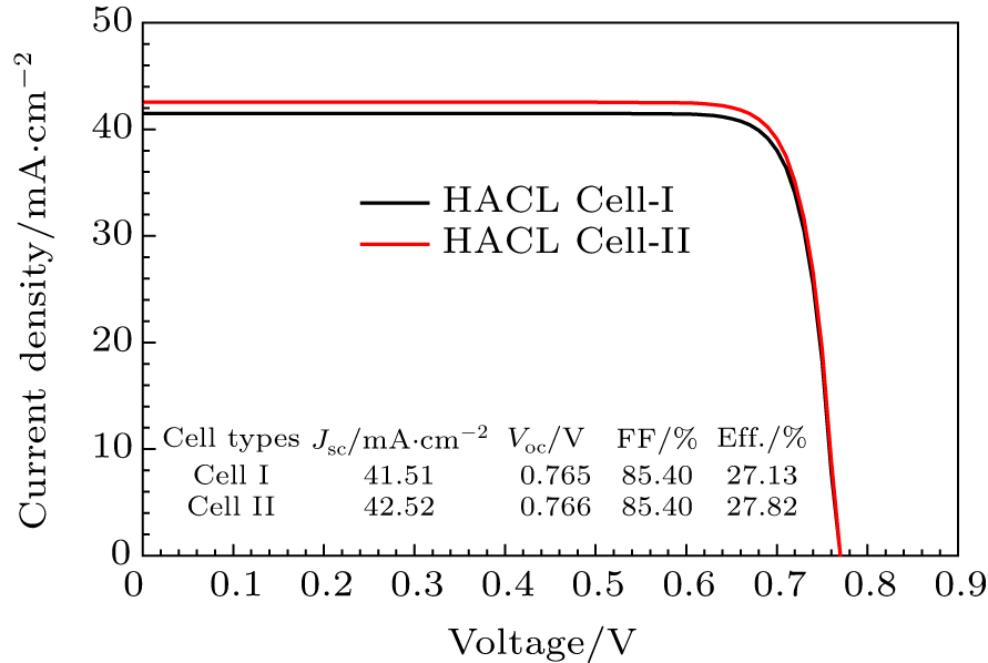 | Fig. 8. Current-voltage curves of the HACL cell-I and cell-II. |
3.4. HACL cell with all n-type c-Si passivating region
It can be seen from Fig.
Similarly, it can be inferred that if the optical absorber of an HACL solar cell is p-type c-Si base, the passivating layers can be all p-type c-Si.
| Table 3. Calculated photovoltaic performance of the HACL cell-III and cell-IV. . |
3.5. TCO-free analysis for HACL cells
For the planar junction, a TCO layer must be deposited on the whole a-Si:H layer to effectively collect the current of solar cells since the lateral conductive property of a-Si:H is weak. However, the TCO layer can be free for our HACL cell. The above simulation results prove that the TCO-free HACL cell can obtain high conversion efficiency. The reason may be that the emitter is local, and its width is small. According to our design, the width of the c-Si passivating region is about 1500 μm, and the width of the a-Si:H emitter is about 50 μm. This small emitter width does not affect the collection of current though the lateral conductive property of a-Si:H is weak.
It is well known that TCO materials contain rare and very expensive metals, such as indium. This makes TCO materials account for about 10% of the cost of the entire cell. TCO-free cells also reduce the number of fabrication steps. Therefore, the TCO-free HACL cell can achieve a reduction in production cost. Moreover, the TCO-free cells can reduce the series resistance loss caused by carrier transport in the TCO. Thus, the HACL structure can also improve cell performance and reduce cell cost by the TCO-free way.
4. Conclusions
A numerical simulation has been carried out using the ATLAS program. The effect of the a-Si:H layer on the performance of the HIT cell is studied. The performance improvement mechanism for the HACL cell is explored. The potential performances of the HIT, HACD and HACL cells are evaluated. It is found that the a-Si:H layer can reduce short-wavelength quantum efficiency and decrease short-circuit current density. The HACL cell can reach a conversion efficiency of 28.18% and a short-circuit current density of 43.06 mA/cm2. The excellent performance for the HACL cell originates from the unique structure design based on local p–n junction. The advantage of the HACL structure is that more photons can be entered into the cell absorber to generate photocarriers since a-Si:H layers are free in the non-junction regions and the collection efficiency of photocarriers can be improved since a very thin passivating layer can reduce photocarrier recombination. The double-side local junction is very suitable for the bifacial solar cells. Furthermore, for an HACL cell with n-type or p-type c-Si base and double-side local junction, all n-type or p-type c-Si passivating layers are feasible for convenience of the double-side diffusion process. Moreover, the TCO materials, in which there is rare and valuable metal element of indium, are free for the HACL structure so that the production cost can be reduced. The results show that the HACL solar cell may be a promising structure for high efficiency and low cost in mass production.
Reference
| [1] | |
| [2] | |
| [3] | |
| [4] | |
| [5] | |
| [6] | |
| [7] | |
| [8] | |
| [9] | |
| [10] | |
| [11] | |
| [12] | |
| [13] | |
| [14] | |
| [15] | |
| [16] | |
| [17] | |
| [18] | |
| [19] | |
| [20] | |
| [21] | |
| [22] | |
| [23] | |
| [24] | |
| [25] | |
| [26] | |
| [27] | |
| [28] | |
| [29] | |
| [30] | |
| [31] |