Multiple enlarged growth of single crystal diamond by MPCVD with PCD-rimless top surface
Ren Ze-Yang, Liu Jun, Su Kai, Zhang Jin-Feng, Zhang Jin-Cheng, Xu Sheng-Rui, Hao Yue
State Key Discipline Laboratory of Wide Band-Gap Semiconductor Technology, School of Microelectronics, Xidian University, Xi’an 710071, China


† Corresponding author. E-mail: jfzhang@xidian.edu.cn

Project supported by the National Key Research and Development Program of China (Grant Nos. 2018YFB0406504 and 2016YFB0400105) and the National Postdoctoral Program for Innovative Talents, China (Grant No. BX20190263).

Abstract

We report the simultaneous enlarged growth of seven single crystal diamond (SCD) plates free from polycrystalline diamond (PCD) rim by using a microwave plasma chemical vapor deposition (MPCVD) system. Optical microscope and atomic force microscope (AFM) show the typical step-bunching SCD morphology at the center, edge, and corner of the samples. The most aggressively expanding sample shows a top surface area three times of that of the substrate. The effective surface expanding is attributed to the utilization of the diamond substrates with (001) side surfaces, the spacial isolation of them to allow the sample surface expanding, and the adoption of the reported pocket holder. Nearly constant temperature of the diamond surfaces is maintained during growth by only decreasing the sample height, and thus all the other growth parameters can be kept unchanged to achieve high quality SCDs. The SCDs have little stress as shown by the Raman spectra. The full width at half maximum (FWHM) data of both the Raman characteristic peak and (004) x-ray rocking curve of the samples are at the same level as those of the standard CVD SCD from Element Six Ltd. The nonuniformity of the sample thickness or growth rate is observed, and photoluminescence spectra show that the nitrogen impurity increases with increasing growth rate. It is found that the reduction of the methane ratio in the sources gas flow from 5% to 3% leads to decrease of the vertical growth rate and increase of the lateral growth rate. This is beneficial to expand the top surface and improve the thickness uniformity of the samples. At last, the convenience of the growth method transferring to massive production has also been demonstrated by the successful simultaneous enlarged growth of 14 SCD samples.

1. Introduction

Due to its exceptional properties, such as wide bandgap, high carrier mobility, high thermal conductivity, extreme hardness, diamond has tremendous advantages to be used as a semiconductor, heat sink, cutting tools, or gems.[15] The single crystal diamond (SCD) has better properties than the polycrystalline diamond (PCD), since it has no grain boundaries. However, the lack of the large diamond substrate blocks the development of the SCD severely. The commercially available SCD plates larger than 5 mm × 5 mm are very expensive. What is more, the growth rate of high quality SCD is usually lower than ten microns per hour.[6] Thus, it is of great interest to develop the methods that could obtain the SCD with high crystal quality, high growth rate, or even multiple growth.[7,8]

Previously the multiple-substrate growth processes including the so-called “mosaic” or “multiple” growth have been developed.[913] In these processes, the substrates are usually placed exactly side by side. However, the PCD rims easily appear at the seams among the substrates during the growth, which induces the shrinkage of the top surface of the grown SCD. Recently, it is found that the pocket-type substrate holder and the constant growth temperature are effective to eliminate the PCD rims during the growth,[14,15] and we also have achieved the laterally enlarged growth of the single crystal diamond by using a microwave plasma chemical vapor deposition (MPCVD) system.[16]

In this paper, we report the simultaneous enlarging growth of the multiple SCD plates by using the MPCVD system. The substrates are placed apart from each other. During growth, the temperature of the SCD surface is kept constant by reducing the height of the substrate without changing any growth parameters. After growth, the expanded SCD surfaces without any PCD rims are achieved, and the property and uniformity of the grown SCDs are investigated.

2. Experiment details

The commercially available high-temperature high-pressure (HTHP) grown type-Ib (001) substrates were used. The size of the substrates is 3 mm × 3 mm × 1.5 mm. Based on our previous investigation,[16] we found that the substrate with four (100) side surfaces can achieve the effective enlargement. Thus, all samples used in this work have (100) top and side surfaces.

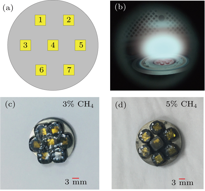
The growth was performed in an MPCVD system with the microwave power and frequency of 6 kW and 2.45 GHz, respectively. Before growth, the substrates were etched in the hydrogen plasma with 2% oxygen added to eliminate the surface defects induced by mechanical polishing, and the surface with low dislocation density was chosen for the growth. Then, we brazed all the substrates on a circular molybdenum holder using 25-μm-thick gold foil to obtain the stable thermal exchange between the substrates and the holder during growth. All molybdenum holders have the same diameter of 20 mm. The samples placed apart from each other are marked as Nos. 1–7, as shown in Fig. 1(a). The purity of the hydrogen and the methane we used is 6N and 5N5, respectively. During growth, the pressure, temperature, and microwave power are 290 mbar, 920 °C, and 3.8 kW, respectively. Figure 1(b) shows the scene of the CVD chamber interior during the multiple SCD growth. To keep the sample surface temperature at a constant level, we reduced the height of the sample by 10 μm when the temperature reached 920 °C. The total gas flow rate of 200 sccm and the methane concentrations of 3% and 5% were used for two batches of samples. After growth, the morphology of the samples was observed by an optical microscope and the Bruker Dimension ICON atomic force microscope (AFM) system. The crystalline quality, stress, and the corporation of impurities of the samples were characterized by using x-ray diffractometry (XRD), Raman and photoluminescence (PL) spectra. The XRD measurements were performed by using the Bruker D8-Discover x-ray diffractometer. The Raman and PL spectra were measured using a confocal Jobin Yvon LavRam HR800 micro-Raman spectrometer with a charge-coupled device (CCD) detector and an optical microscopy system. The wavelength of the excitation laser is 514 nm. All characterizations were performed at room temperature.

Fig. 1. (a) Schematic diagram of the substrate locations on the molybdenum holder and (b) interior scene of the CVD chamber during growth. (c) and (d) The as-grown samples with (100) side surfaces.
3. Results and discussion

The as-grown samples using different CH4 densities of 3% and 5% are shown in Figs. 1(c) and 1(d). Note that the two batches of samples are grown on the holders with the same size. It can be observed that the as-grown samples have a much larger top surface compared with the substrates (see the yellow color). That is, the enlarged growth of SCD has been achieved for all the samples. The epilayer thickness and the growth rate are listed in Table 1. The growth rates of different samples on the same holder are different, and the central one always has the lowest growth rate. This may be induced by the slight temperature difference among different samples and the ununiform spacial distribution of carbon species in the gases.

Table 1.

Summary of the thickness and growth rate of the diamond epilayers.

.

With the decreasing methane density, the growth rate apparently decreases. For the samples grown with 3% CH4 density, the lateral growth leads to the side connection among the samples after the long time growth. However, we can observe that there is still no PCD appearing in the connecting interfaces between the samples. However, some bulges can be observed around the sample sides due to generation of defects and related abnormal nucleation/growth, and this is completely different from the PCD rims. One can also find that the ratio of the growth rate in the batch of samples could reach a maximum of 15.2/8.6 = 177% for the samples grown with 5% methane and 6.7/5.2 = 129% for the samples grown with 3% methane. This indicates the thickness nonuniformity of the latter is much smaller compared with that of the former. As a result, proper reduction of the methane ratio in the sources gas flow in the multiple growth of CVD SCDs by our method is beneficial to expand the top surface and improve the thickness uniformity of the samples.

As above mentioned, we can maintain the temperature of the SCD surfaces almost constant by only decreasing the sample height, and thus all the other growth parameters (microwave power, pressure, etc.) can be kept unchanged. As shown in Fig. 2, during growth the sample holder height is decreased when the CVD layer grows thicker. This variation of the height is controlled automatically by our MPCVD system. We set the height descent step and the sample surface temperature at 10 μm and 920 °C, respectively. Once the temperature of the sample surface reaches 920 °C, the holder height decreases by 10 μm. It can be observed from Fig. 2 that height decreasing averagely occurs every 1.6 h for the samples grown with 3% CH4 density, and every 0.9 h for the samples grown with 5% CH4 density. Therefore the average decreasing rates are 6.2 μm/h and 11.1 μm/h for the samples grown with 3% and 5% CH4 density, respectively, and are almost the same with the average growth rates of 6.0 μm/h and 12.1 μm/h. Thus, the sample surfaces have almost a constant height during the whole growth process. The constant growth temperature can be achieved by no variation of any other growth parameters.

Fig. 2. Sample holder height versus growth time for the samples grown with (a) 3% and (b) 5% CH4 density.

The maintenance of the constant temperature at the sample surface has been reported to be very important to obtain high quality and PCD rimless SCD, and has realized by continuously decreasing the input microwave power.[15] However, this method is in principle not suitable for multiple growth because the decrease of the microwave power will cause the compression of the plasma and aggregate the growth nonuniformity among samples. Moreover, the change of the growth parameter easily leads to the change of impurity incorporation or lattice constant, then induces the internal stress or defects. Compared to the reported method in Ref. [15], our method does not change any growth parameters. Thus, little internal stress or dislocations would be induced. Figure 3 gives the XRD (004) 2θω results of the samples grown with and without constant growth parameters. The sample grown with the changing parameters (Fig. 3(b)) shows the asymmetric diffraction peak, which indicates an inner stress existing in the sample.
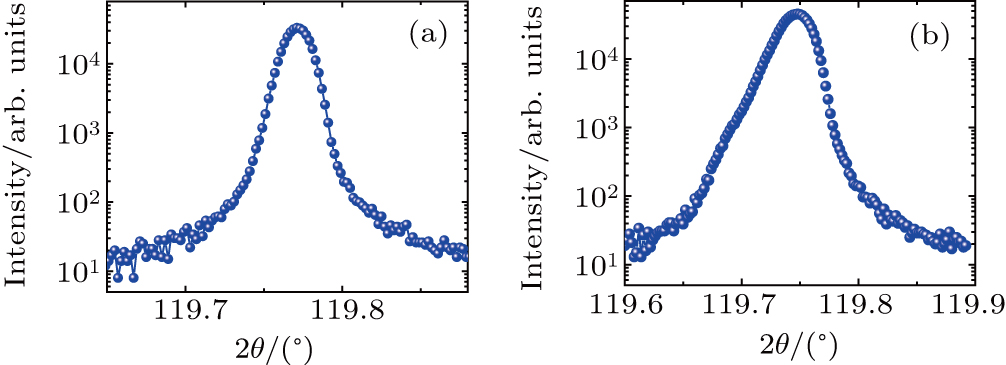
Fig. 3. The XRD (004) 2θω results of the CVD SCDs (a) with and (b) without constant growth parameters.

The surface morphologies of the as-grown samples of both batches (Fig. 4) are similar, and feature the typical step bunching morphology commonly found for CVD SCDs.[17] In addition, we can see that the samples grown with 3% methane have less bulges on the surfaces than those with 5% methane. We further characterized the morphology of the step bunching by using AFM. The results are shown in Fig. 5. The samples grown with 3% and 5% CH4 density have almost the same depth of the step bunching.

Fig. 4. Surface morphology of the diamond samples grown with (a)–(g) 3% methane and (h)–(n) 5% methane, and (o) surface morphology near an edge of the as-grown diamond (bottom right) between two truncated corners.
Fig. 5. AFM morphologies of the samples grown with (a) 3% and (b) 5% CH4 density.

Figure 4(o) shows that the step bunching extends directly to the edges of the sample, which indicates that the whole top surface is SCD and no PCD rims appear. However, the shrinkage of the top surface compared with the measured largest part of the sample occurs due to the four truncated corners. This is similar to the result reported in Ref. [18] and can be explained by the development of the (113) faces at the corners. The (113) faces have a slowest growth rate in SCD growth, and are prone to twinning and defect nucleation inducing stress and cracks at the corners. After cutting and polishing, the substrates (in yellow color) and the CVD SCDs are shown in Fig. 6(a), and the latter after substrate removal and polishing generally shows highly defective corners with cracks. All CVD grown samples show good brightness. The yellow color in some of the CVD SCDs comes from the residuum of the substrate. It can be seen clearly that the CVD plates are larger than the substrates. Usually the imperfect crystal has been cut off, so the CVD plates are smaller than the as-grown ones. However, the maximum sample in Fig. 6(a) still has the edge-to-edge distance of 5.6 mm, which corresponds to the effective area of above 30 mm2. This value indicates more than three times enlargement of the top surface after the growth has been achieved.

Fig. 6. (a) Picture of the substrates and the CVD SCDs and (b) the positions of the Raman characteristic peak of diamond of both batches of CVD SCDs.

We measured the Raman spectra of the samples to characterize the stress in the CVD SCDs. For all the samples, the Raman characteristic peak of diamond[19] appears near 1332.5 cm−1 (Fig. 6(b)), and except this very strong peak no other peaks appear. This indicates the low stress and the good uniformity of the SCDs. The full width at half maximum (FWHM) of the Raman peak ranges from 3.0 cm−1 to 3.4 cm−1, as a reference that of the standard CVD SCD from Element Six Ltd measured by the same Raman system is over 3.0 cm−1. So our samples are of similar quality. In addition, we find that the measured FWHM data are associated with the optical grating used in the Raman system. If the grating changes from 1800 g/mm to 2400 g/mm, the FWHM of the same sample will decreases from 3.0 cm−1 to 1.8 cm−1 typically reported for high quality SCDs.[10]

In order to investigate the incorpration of nitrogen and optical properties of the samples, the PL spectra were measured (Fig. 7). In our experiment, we grew the SCD without using any gas purifier, and the unintentionally introduced nitrogen may come from the hydrogen produced by water decomposition. The peak at 552 nm related to Raman peak R and the typical PL peaks at 575 nm and 638 nm, related to (NV)0 and (NV), respectively, are observed for both series of samples.[20] Meanwhile, there is an intense broad band ranging from 600 nm to 800 nm, which was considered as the associated phonon replicas of NV-related zero phonon lines.[20] One can find that the intensity of the broad band increases with the increase of the growth rate. For the samples grown with the methane density of 3%, the intensity of the broad band is weaker than that of Raman peak R. However, it is stronger than Raman peak R for the sample grown with 5% methane density. The intensities of the NV-related peak and the broad band are positively correlated with the nitrogen density in the sample. Thus, we can conclude that the incorporation of nitrogen impurity increases with increasing growth rate. Especially for the samples grown with the same CH4 density, the sample placed at the center of the holder (i.e., at position 4) always has the minimum growth rate and weakest PL band intensity ranging from 600 nm to 800 nm, so it has the lowest nitrogen density in the batch of samples.
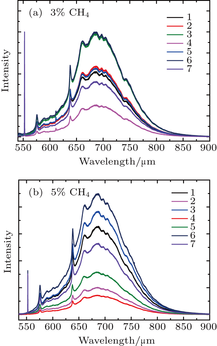
Fig. 7. Results of PL measurement for the samples grown with the CH4 densities of (a) 3% and (b) 5%.

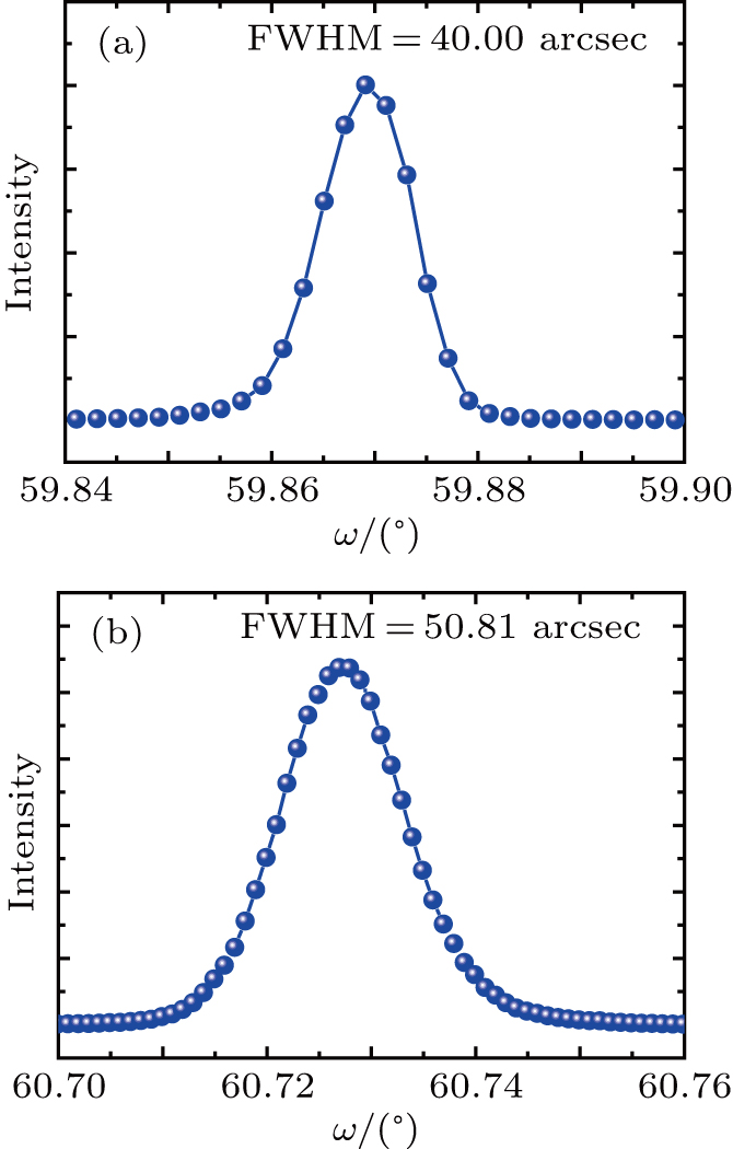
We also used XRD to characterize the crystalline quality of the samples grown with different CH4 density. The typical results are shown in Fig. 8. The FWHMs of the (004) rocking curves are measured to be 40.00 arcsec and 50.81 arcsec for the samples grown with 3% and 5% CH4 density, respectively. The FWHM data of both batches of samples are comparable with that of the standard CVD SCD from Element Six Ltd (over 40 arcsec), and they also indicate that the quality of the 3% CH4 grown sample is slightly better than the 5% grown ones.

Fig. 8. XRD results of the samples grown with (a) 3% and (b) 5% CH4 density.

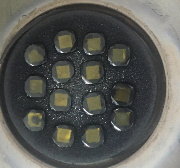
As a further demonstration of the multiple growth ability, we also achieved the simultaneous growth of over ten SCD samples. Figure 9 shows the growth of 14 samples by using the method introduced in this paper. These samples were grown with 5% CH4 and had the same growth parameters with the above mentioned 7 pieces samples. The holder has a customized dimension of 35 mm in diameter. After a growth time of 57 h, all the samples had achieved effective enlargement. Based on these results, we suggest that this method of multiple enlarged growth of SCDs can be further extended to the simultaneously enlarged growth of dozens or even hundreds of samples, if the MPCVD system with 915 MHz could be used in the future.

Fig. 9. Demonstration of the multiple enlarged growth of 14 SCD samples.
4. Conclusion and perspectives

We have achieved the simultaneous enlarged growth of seven SCD samples by using an MPCVD system and investigated their properties. The substrates are brazed on a pocket holder to achieve the stable and uniform heat exchange, and separated from each other to allow the sample surface expanding. After the growth at almost a constant temperature, all the diamond plates have larger and PCD-rimless top surfaces clarified by the typical step-bunching SCD morphology at the center, edge, and corner of the samples observed by optical microscope and AFM. The most aggressively expanding sample shows a top surface area three times of that of the substrate. The SCDs have little stress as shown by the Raman spectra. The FWHM data of both the Raman characteristic peak and (004) XRD rocking curve of the samples are at the same level as those of the standard CVD SCD from Element Six Ltd, which hints the high quality of our samples. The nonuniformity of the sample thickness or growth rate is observed, and PL spectra show that the nitrogen impurity increases with increasing growth rate. We also find that proper reduction of the methane ratio in the sources gas flow is beneficial to expand the top surface and improve the thickness uniformity of the samples. At last, the convenience of the growth method transferring to massive production has also been demonstrated by the successful simultaneous enlarged growth of 14 SCD samples.

Reference
[1] Isberg J Hammersberg J Johansson E Wikstrom T Twitchen D J Whitehead A J Coe S E Scarsbrook G A 2002 Science 297 1670
[2] Achard J Silva F Tallaire A Bonnin X Lombardi G Hassouni K Gicquel A 2007 J. Phys. D: Appl. Phys. 40 6175
[3] Yan C S Vohra Y K Mao H K Hemley R J 2002 Proc. Natl. Acad. Sci. USA 99 12523
[4] Wang J K Li S S Wang N Liu H J Su T C Hu M H Han F Yu K P Ma H A 2019 Chin. Phys. Lett. 36 046101
[5] Chayahara A Mokuno Y Horino Y Takasu Y Kato H Yoshikawa H Fujimori N 2004 Diamond Relat. Mater. 13 1954
[6] Bolshakov A P Ralchenko V G Yurov V Y Popovich A F Antonova I A Khomich A A Ashkinazi E E Ryzhkov S G Vlasov A V Khomich A V 2016 Diamond Relat. Mater. 62 49
[7] Zhao Y Guo Y Lin L Zheng Y Hei L Liu J Wei J Chen L Li C 2018 J. Cryst. Growth 491 89
[8] Liu J Lin L Zhao Y Zheng Y An K Wei J Chen L Hei L Wang J Feng Z Li C 2018 Vacuum 155 391
[9] Geis M W Efremow N N Susalka R Twichell J C Snail K A Spiro C Sweeting B Holly S 1994 Diamond Relat. Mater. 4 76
[10] Tallaire A Achard J Secroun A De Gryse O De Weerdt F Barjon J Silva F Gicquel A 2006 J. Cryst. Growth 291 533
[11] Yamada H Chayahara A Y Kato Y Shikata S 2014 Appl. Phys. Lett. 104 102110
[12] Yamada H Chayahara A Mokuno Y Tsubouchi N Shikata S Fujimori N 2011 Diamond Relat. Mater. 20 616
[13] Asmussen J Grotjohn T A Schuelke T Becker M F 2008 Appl. Phys. Lett. 93 031502
[14] Nad S Asmussen J 2016 Diamond Relat. Mater. 66 36
[15] Charris A Nad S Asmussen J 2017 Diamond Relat. Mater. 76 58
[16] Ren Z Y Zhang J F Zhang J C Xu S R Zhang C F Su K Li Y Hao Y 2018 Chin. Phys. Lett. 35 078101
[17] Yamada H Chayahara A Mokuno Y 2016 Jpn. J. Appl. Phys. 55 01AC07
[18] Tallaire A Achard J Silva F Brinza O Gicquel A 2013 CR Phys. 14 169
[19] Prawer S Nemanich R J 2004 Philos. Trans. R. Soc. London Ser. A-Math. Phys. Eng. Sci. 362 2537
[20] Li H D Zou G T Wang Q L Cheng S H Li B Lue J N Lue X Y Jin Z S 2008 Chin. Phys. Lett. 25 1803