Single-electron transport through single and coupling dopant atoms in silicon junctionless nanowire transistor
Project supported by the National Key R&D Program of China (Grant No. 2016YFA0200503).
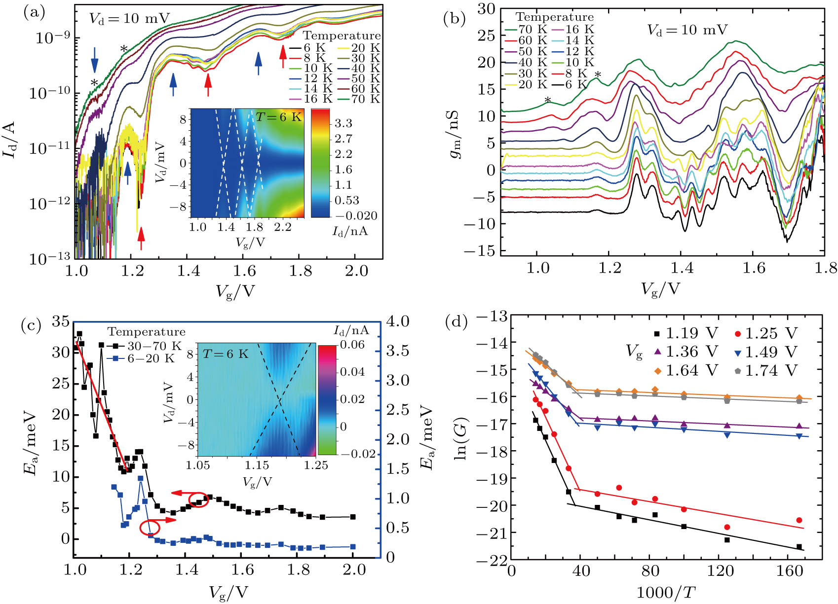
(a) Temperature dependence of Id–Vg characteristics (Vd = 10 mV) for silicon JNT (6–70 K). Inset: stability diagram of drain current Id vs. gate and bias voltages at T = 6 K. (b) The transconductance gm versus gate voltage Vg with Vd = 10 mV from 6 K to 70 K. The transconductance curves have been shifted by an offset 2 nS for clarity. (c) Activation energy Ea estimated from Arrhenius plots as a function of Vg at Vd = 10 mV in two different temperature regions. Inset: the current range narrowed less than 0.06 nA for the stability diagram in the inset of (a) for clarify at the low Vg. (d) The Arrhenius plots of conductance at various gate voltages corresponding to the marked Vg by arrows in (a).
