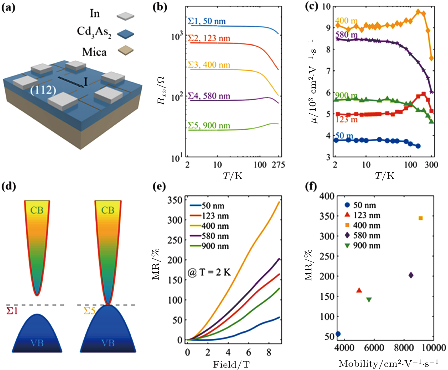
Electrical transport and optical properties of Cd3As2 thin films
(a) Schematic diagram of standard six-probe Hall bar fabricated on Cd3As2 thin films with mica substrate, used for transport measurements in the PPMS system. Crystal orientation is (112), which is perpendicular to the magnetic field (up to 9 T). (b) Zero-field temperature-dependent longitudinal resistance Rxx curves for five Cd3As2 thin films with different thicknesses ranging from 50 nm to 900 nm; Rxx drops with sample thickness reducing, indicating a thickness-induced insulator-to-metal transition. (c) Variations of carrier mobility μ with temperature. Carrier mobility is about
