|
Guo Yang-Yan1, 2, Han Wei-Hua1, 2, †, Zhao Xiao-Song1, 2, Dou Ya-Mei1, 2, Zhang Xiao-Di1, 2, Wu Xin-Yu1, 2, Yang Fu-Hua1, 2, 3
|
|
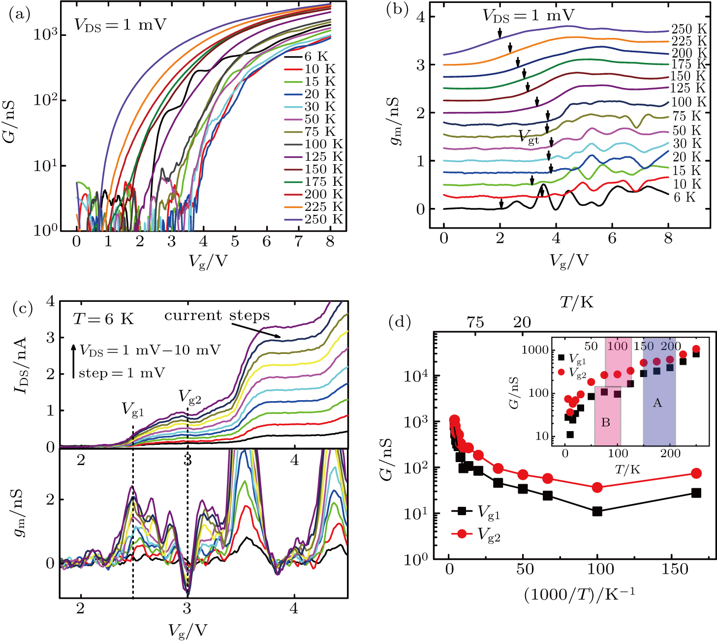
(a) The temperature-dependent conductance G (i.e., G = IDS/VDS) curves of the device at VDS = 1 mV within the temperature range from 6 K to 250 K. (b) The temperature-dependent transconductance gm–VG characteristics at VDS = 1 mV, where the transconductance is given by
g
m
=
d
I
DS
/
d
V
G
. (c) IDS–Vg curves (upper part) and the corresponding transconductance gm–Vg curves (lower part) at the temperature of 6 K under the bias VDS varying from 1 mV to 10 mV. (d) The Arrhenius conductance plots (G vs. 1/T) on logarithmic scale at the gate voltages of Vg1 and Vg2 within the temperature range from 6 K to 250 K, The inset shows the corresponding temperature-dependent conductance data (G vs. T), which are extracted from panel (a) after unified by the onset gate voltage Vgt at different temperatures.
|
