Charge trapping memory device based on the Ga2O3 films as trapping and blocking layer
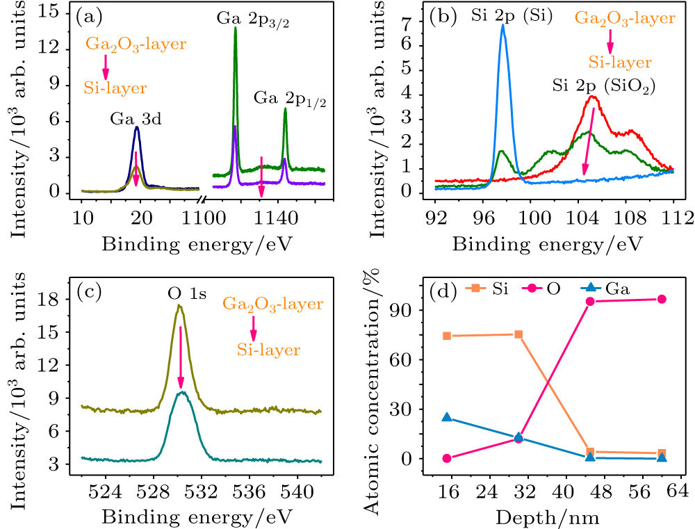
XPS depth analysis of the device annealed at 760 °C: (a) Ga 2p3/2, 2p1/2, and 3d spectrum, (b) Si 2p spectrum, (c) O 1s spectrum, and (d) atom concentration with various depths from Ga2O3 to Si layers.
