Negative gate bias stress effects on conduction and low frequency noise characteristics in p-type poly-Si thin-film transistors
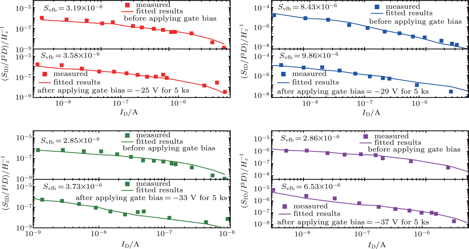
Curves of normalized noise versus drain current power spectral density before and after NBS (VDS = −0.5 V).
Negative gate bias stress effects on conduction and low frequency noise characteristics in p-type poly-Si thin-film transistors |
|
Curves of normalized noise versus drain current power spectral density before and after NBS (VDS = −0.5 V). |
| |