Monolithic semi-polar (
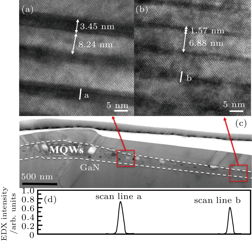
(a) and (b) High-magnification cross-sectional TEM images of MQW portion, which corresponds to different parts (red squares) of panel (c). (c) TEM of MQWs portion revealing individual InGaN/GaN QWs. Dashed lines indicate the boundaries of the MQWs. (d) TEM-EDX lines scanning in direction perpendicular to QW: Line a and line b representing the center and the side of the stripe, respectively.
