1. IntroductionAt present, III–V compound semiconductors provide the material basis for a number of well-established commercial technologies, and have applications in electronic and optoelectronic devices,[1] especially in lasers,[2] light-emitting diodes (LEDs),[3] solar cells,[4] and photodetectors.[5] During the past decades, most research has been done with III–V material systems. Kim et al. have studied the elastic constants and related properties of tetrahedrally bonded BN, AlN, GaN and InN systematically, and they obtained some important conclusions about the four binary alloys.[6] In 1999, Kern et al. obtained the phase diagram of boron nitride via ab initio calculation.[7]The band parameters for 13 kinds of III–V semiconductor alloys have been calculated in Ref. [1] with the
 method. However, all of the studies were mainly engaged in the bulk phase of III–V materials.[8] In 2004, Novoselov et al. produced graphene by mechanical exfoliation of graphite and proved many excellent properties existing in this strict two-dimensional (2D) monolayer material.[9] From then on, more and more research has been focused on the free-standing 2D material systems, both theoretically and experimentally.[10–14] In 2D III–V material systems, BN[14,15] and phosphorene[16–18] are the most intensively studied ones; GaN, AlN, GaAs, GaSb, and GaP are also studied by researchers,[19–21], who have proven that the physical properties of III–V alloys would be very different from those of bulk ones. Based on density functional theory (DFT), many aspects have been studied for 2D III–V materials, such as the effects of the strain and external electric field on the electronic properties,[20] intrinsic defect formation energy in BN bilayer and monolayer,[22] the tuning of the band gap of InxGa1−xN by changing the number of layers,[23] the mechanical anisotropy and lattice defects of borophene,[24] and the structural and electronic properties of B2 N3.[25] These studies, which mainly focus on some important physical properties of one or several kinds of III–V2D materials in the case of some external factors, are introduced. To the best of our knowledge, few publications are found to compare and study the regularity of certain properties systematically under the conditions with or without stress for all 25 kinds of III–V2D binary alloys AB (A = boron, aluminum, gallium, indium, thallium, and B = nitrogen, phosphorus, arsenic, Sb (antimony), bismuth). We speculate that by comparing these 25 kinds of 2D materials together, some important regularities behind the physical properties could be found more clearly and intuitively, significant for finding some new 2D materials used in various fields, as well as guiding the experimenters in choosing the combinations of two or more elements which would prepare better material. Motivated by this, we calculate all III–V2D materials by first-principles method. The remainder of this paper is organized as follows, methodology and computational details are described in Section 2. In Section 3 the calculations of band structures, effective mass of electrons and holes at band edges and elastic properties are presented. Finally, some conclusions are briefly summarized in Section 4.
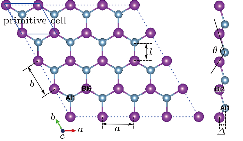
3. Results and discussion3.1. Structural propertiesIn order to clearly describe the structures used in this paper, a 4 × 4 AlBi supercell is used as a template structure and illustrated in Fig. 1. We note that all other 24 kinds of binary alloys have a similar structure as shown in Fig. 1 and for all calculations the primitive cell is used.
The calculated lattice constant (a), bond length (l), buckling constant (Δ), bond angle (θ), formation energy (Ef), band gap (Eg), effective mass of electrons (
 ), effective mass of holes (
 ) and the band gap types (D/ID), where D and ID represent the direct and indirect energy band gap respectively, are listed in Table 1 and divided into five groups according to the V atoms. One can find that for III–V binary compounds (III = B, Al, Ga, In, Tl, V = N, P, As, Sb, Bi), both the lattice constant and bond length increase unsurprisingly with the radius of atom increasing, and the lattice parameters of GaN, GaP, GaAs, and GaSb are consistent with those in Refs. [20] and [36] with a small error of less than 1%, and the lattice constant of bulk h-BN in Ref. [37] from first principles method is 2.494 Å, which is underestimated only by 0.7% compared with our results. According to our calculations, of 25 kinds of binary III–V compounds, 7 kinds of binary compounds have a planar structure similar to graphene. i.e., BN, AlN, GaN, InN, BP, BAs, and BSb are optimized into a planar monolayer structure, and the results are in compliance with those in Ref. [38]; in addition, TlN and AlP are very inclined to forming flat structures with a bond angle 119.921° and 119.407° respectively. It can be concluded that the smaller the lattice constant, the easier the planar structure to be formed. To be more precise, the lattice constant and bond length of a planar monolayer must be smaller than 3.74 Å and 2.16 Å for an III–V binary respectively. We note that all XN (X = B, Al, Ga, In, Tl) and BY (Y = N, P, As, Sb, except for Bi) 2D compounds tend to be planarized due to the lattice constants and bond lengths are smaller than 3.74 Å and 2.16 Å respectively. Conversely, there are 16 kinds of III–V compounds with a buckling structure due to a larger dimension and the buckling constant (Δ) that represents the degree of buckling. Also, we calculate the formation energy for all binary compounds from the following formula:
 | |
where

,

,

, and

are the formation energy, energy of monolayer
III–
V binary,
III atom energy, and
V atom energy respectively, the formation energy of GaN, GaP, GaAs, and GaSb are −8.122, −5.201, −4.391, and −3.870 eV,
[20] respectively and are very close to our results in Table
1. Obviously, the formation energy in the same group (
i.e., a given
V atom) and different groups (
i.e. a given
III atom) both increase with the increase of radii of
V and
III atoms. As a more negative formation energy means a more favored stable structure, a conclusion can be drawn that a smaller atom is beneficial to not only the formation of a planar structure, but also to a layered 2D structure, which is consistent with the results of mechanical properties as shown in the next section. As analyzed above, that the
III–Ns and B–
Vs (except for BBi) are favored in energy to form a planar monolayer can be explained by the fact that they have a smaller formation energy. = 14.0pt plus.2pt minus.2pt
3.2. Mechanical propertiesWe calculate the mechanical parameters such as stiffness constants Cij(
 ), i,j = 126 Young’s modulus Yk
 k = x,y, shear modulus S (GPa, nm, N/m), and Poisson’s ratio of all 25 kinds of III–V binary 2D monolayers. For a 2D structure, the relation between stress and strain can be derived based on Hooke’s law under in-plane stress conditions as follows:[24]
Here,
Cij is the second partial derivative of strain energy
Es with respect to strain
ε, corresponding to the component of the elastic modulus tensor, and can be written as
S
0 is the equilibrium area of the crystal. In a general way used in ab-initio calculations for a 2D material,
Es is determined by formula (
4) using the standard Voigt notation,
[39]In the calculations, we define the strain

and
b0 as the lattice constant with and without strain, respectively. For the uniaxial and equi-biaxial strain, we apply a finite scaling to the

and

direction, where

is chosen to be along lattice

vector (zigzag) and

(armchair) to be perpendicular to

. The most favorable structure in energy is set to be the strain-free structure and the strain range along the corresponding direction changes from −2.5% to 2.5% in steps of 0.5%. The shear strain is also considered in this paper, which means that we will do the calculations 44 times for each binary monolayer in order to obtain the elastic constants by fitting the data of elastic strain energy
Es(
ε) as a function of strain
ε using a quadratic polynomial. After that, the Young’s modulus
Y and Poisson’s ratio
υ can be derived as
[40]
Noting that the shear modulus (
S) of a 2D crystal can be obtained directly based on
C66 (
S =
C66), by using a post-processing VASPKIT code,
[33] the stiffness constants, Young’s modulus, shear modulus and Poisson’s ratio are obtained as listed in Table
2.
Table 2.
Table 2.
 Table 2.
Calculated elastic stiffness constants Cij (GPa, nm, N/m), i,j = 126, Young’s modulus Yk (
 , N/m), k = xy, shear modulus S (GPa, nm, N/m), and Poisson’s ratio νk, k = x,y.
.
| Monolayer |
Stiffness tensor/(N/m) |
Young’s modulus/(N/m) |
Shear modulus/(N/m) |
Poisson’s ratio |
|
|
|
|
|
|
C11 |
C22 |
C12 |
C66 |
Yx |
Yy |
S |
νx |
(νy |
| BN |
290.666, 293.1[42] |
290.085 |
65.277, 63.76[42] |
112.873 |
275.977, 279.2[42] |
275.425 |
112.873 |
0.225, 0.21[38] |
0.225 |
| AlN |
143.792 |
142.948 |
66.227 |
39.176 |
113.109 |
112.446 |
39.176 |
0.463, 0.46[38] |
0.461 |
| GaN |
133.201, 110[38] |
132.277 |
59.335 |
37.871 |
106.586 |
105.846 |
37.871 |
0.449 |
0.445 |
| InN |
92.875 |
93.687 |
54.113 |
20.648 |
61.619 |
62.158 |
20.648 |
0.578, 0.59[38] |
0.583 |
| TlN |
61.986 |
61.857 |
85.102 |
9.645 |
−55.095 |
−54.98 |
9.645 |
1.376 |
1.373 |
| BP |
150.788 |
151.17 |
41.777 |
54.491 |
139.243 |
139.596 |
54.491 |
0.276, 0.28[38] |
0.277 |
| AlP |
71.423 |
71.261 |
22.325 |
19.846 |
64.429 |
64.283 |
19.846 |
0.313 |
0.313 |
| GaP |
64.38 |
64.822 |
19.75 |
21.397 |
58.363 |
58.763 |
21.397 |
0.305 |
0.307 |
| InP |
46.792 |
46.459 |
17.867 |
14.254 |
39.92 |
39.637 |
14.254 |
0.385 |
0.382 |
| TlP |
36.816 |
37.083 |
29.372 |
10.679 |
13.553 |
13.651 |
10.679 |
0.792 |
0.798 |
| BAs |
126.279 |
126.115 |
35.591 |
45.589 |
116.235 |
116.084 |
45.589 |
0.282, 0.29[38] |
0.282 |
| AlAs |
53.004 |
53.006 |
18.124 |
17.186 |
46.807 |
46.809 |
17.186 |
0.342 |
0.342 |
| GaAs |
48.981, 48[38] |
48.871 |
16.009 |
16.473 |
43.737 |
43.638 |
16.473 |
0.328 |
0.327 |
| InAs |
36.969, 33[38] |
36.751 |
14.171 |
11.122 |
31.505 |
31.319 |
11.122 |
0.386 |
0.383 |
| TlAs |
26.16 |
26.022 |
15.22 |
6.571 |
17.258 |
17.167 |
6.571 |
0.585 |
0.582 |
| BSb |
94.084 |
94.823 |
31.101 |
32.942 |
83.883 |
84.542 |
32.942 |
0.328, 0.34[38] |
0.331 |
| AlSb |
37.249, 35[38] |
37.176 |
11.844 |
11.98 |
33.475 |
33.41 |
11.98 |
0.319 |
0.318 |
| GaSb |
32.529 |
32.986 |
12.821 |
11.329 |
27.546 |
27.933 |
11.329 |
0.389 |
0.394 |
| InSb |
28.184 |
28.68 |
9.306 |
8.421 |
25.164 |
25.608 |
8.421 |
0.324 |
0.33 |
| TlSb |
21.472 |
20.627 |
39 |
5.182 |
−52.265 |
-50.207 |
5.182 |
1.891 |
1.816 |
| BBi |
66.924 |
66.724 |
19.788 |
23.584 |
61.055 |
60.873 |
23.584 |
0.297 |
0.296 |
| AlBi |
31.055 |
31.266 |
11.563 |
9.819 |
26.779 |
26.961 |
9.819 |
0.37 |
0.372 |
| GaBi |
20.898 |
20.971 |
20.781 |
6.096 |
0.305 |
0.306 |
6.096 |
0.991 |
0.994 |
| InBi |
24.808 |
24.421 |
10.21 |
6.747 |
20.539 |
20.219 |
6.747 |
0.418 |
0.412 |
| TlBi |
17.241 |
17.077 |
12.489 |
3.524 |
8.108 |
8.031 |
3.524 |
0.731 |
0.724 |
| Table 2.
Calculated elastic stiffness constants Cij (GPa, nm, N/m), i,j = 126, Young’s modulus Yk (
 , N/m), k = xy, shear modulus S (GPa, nm, N/m), and Poisson’s ratio νk, k = x,y.
. |
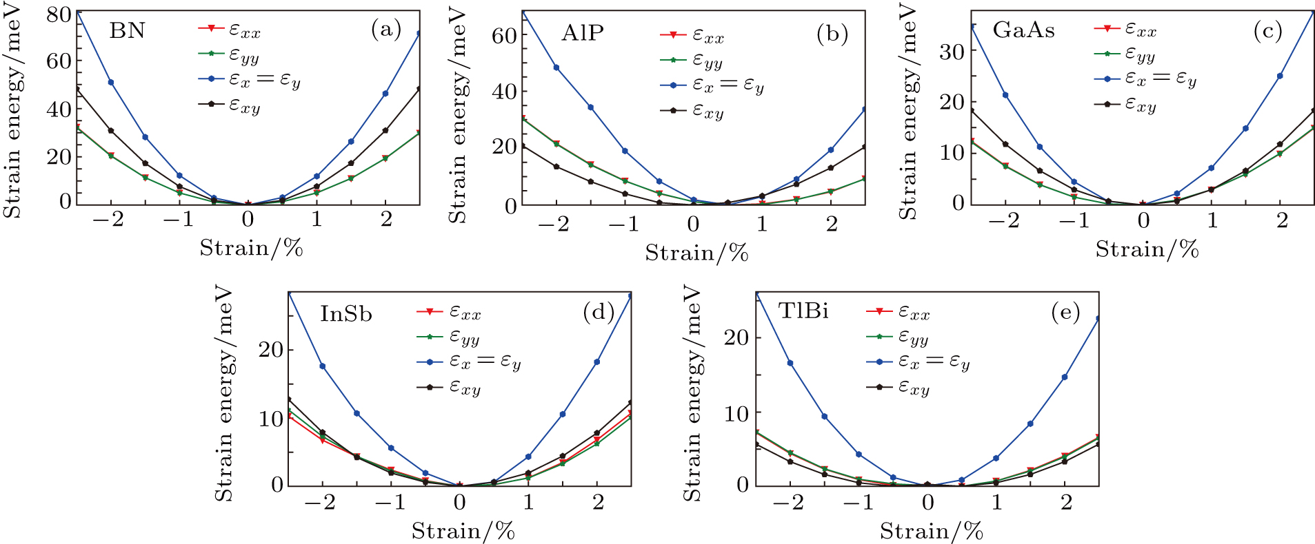
For simplicity, we choose five kinds of binary monolayers as representatives, and the curves of strain-energy versus strain are presented in Fig. 2, i.e., BN, AlP, GaAs, InSb, TlBi are intentionally chosen to include all elements in III–V column, and the
 ,
,
 ,
,
 , and
, and
 are the uniaxial strain in the x direction, the uniaxial strain in the y direction, the equi-biaxial strain, and the shear strain respectively. It can be seen from Fig. 2 that the strain energy values of all binary compounds are almost symmetrical for compression (−2.5% to 0) and tension (0 to 2.5%) for all types of strain except that for AlP, and the non-symmetrical results of strain energy are found in GaBi, AlSb, and BP as well as among other 20 kinds of monolayers (not shown here). The results for BN in the same strain range are in accord with those of Ref. [41], where the total strain range is much larger than ours, and it shows that the symmetry is broken in a larger strain region. The results also show that all monolayer structures, except for InSb, under a small strain are isotropic due to the same strain energy response to the strain in the x direction and that in the y direction. The stiffness of C11, C12, and Young’s modulus in Ref. [41] are, respectively, 293.1, 63.76, and 279.2 (N/m), which are much more consistent with our results listed in Table 2. The Poisson’s ratio and stiffness of BN, BP, AlAs, etc. as listed in Table 2 are also in agreement with those of in Ref. [38], which means that our calculations are convincing and some regularity hence can be concluded by comparing all 25 kinds of binary compounds. Firstly, all mechanical constants except Poisson’s ratio for all cases decrease with the increase of atom radius, i.e., for a given group III element and changing of a group V element into a larger one or smaller one, the mechanical property is very sensitive to the dimension of lattice. Secondly, it is noteworthy that Young’s modulus varies over a large range, i.e., from a minimum value 0.306 N/m for GaBi to a maximum value 275.977 N/m for BN, which means that we can tune the mechanical property of 2D III–V binary materials very flexibly by combining different III–V elements into a binary compound or by dosing different elements into a binary compound to improve the elastic nature. For a mechanically sTable 2D sheet, the Young’s modulus and shear modulus must be larger than zero, i.e.,
 and
and
 . Based on the simple criteria, TlSb and TlN with a Young’s modulus of −55 N/m and −52 N/m respectively are the only two mechanically unstable binary compounds in III–V; at least they are less stable than other binary monolayer structures if the calculation error is taken into consideration. In order to investigate the qualitative relation between an atomic radius and the elastic constant, we assume the relative radius of B, Al, Ga, In, and Tl to be 5, 13, 31, 49, 81 and 7, 15, 33, 51, 83 for N, P, As, Sb, and Bi respectively. The reason for making the above assumption of relative radius for each element can be simply understood from the relative location in the periodic table. Based on the assumption, the radii of all binary compounds are summarized in Table 3.
Table 3.
Table 3.
 Table 3.
Assumed relative radius of each element and binary monolayer.
.
| Binary |
radius |
|
N(7) |
P15) |
As(33) |
Sb(51) |
Bi(83) |
| BN |
12 |
|
|
|
|
|
| AlN |
20 |
|
|
|
|
|
|
| BP |
20 |
|
|
|
|
|
|
| AlP |
28 |
|
|
|
|
|
|
| GaN |
38 |
B(5) |
BN12 |
BP20 |
BAs38 |
BSb 56 |
BBi 8 |
| BAs |
38 |
|
|
|
|
|
|
| GaP |
46 |
|
|
|
|
|
|
| AlAs |
46 |
|
|
|
|
|
|
| InN |
56 |
Al(13) |
AlN20 |
AlP28 |
AlA 46 |
AlSb64 |
AlB 96 |
| BSb |
56 |
|
|
|
|
|
|
| InP |
64 |
|
|
|
|
|
|
| GaAs |
64 |
|
|
|
|
|
|
| AlSb |
64 |
|
|
|
|
|
|
| InAs |
82 |
Ga(31) |
GaN 38 |
GaP 46 |
GaAs 64 |
GaSb 82 |
GaBi 114 |
| GaSb |
82 |
|
|
|
|
|
|
| TlN |
88 |
|
|
|
|
|
|
| BBi |
88 |
|
|
|
|
|
|
| TlP |
96 |
In(49) |
InN56 |
InP64 |
InAs82 |
InSb100 |
InBi132 |
| AlBi |
96 |
|
|
|
|
|
|
| InSb |
100 |
|
|
|
|
|
|
| TlAs |
114 |
|
|
|
|
|
|
| GaBi |
114 |
Tl(81) |
TlN88 |
TlP96 |
TlAs114 |
TlSb132 |
TlBi164 |
| TlSb |
132 |
|
|
|
|
|
|
| InBi |
132 |
|
|
|
|
|
|
| TlBi |
164 |
|
|
|
|
|
|
| Table 3.
Assumed relative radius of each element and binary monolayer.
. |
It is interesting that the relative radii of 25 kinds of binary compounds form a perfect symmetric matrix, e.g., AlN and BP, GaN, and BAs., which are symmetric about the main diagonal with a relative radius of 20 and 38, respectively.
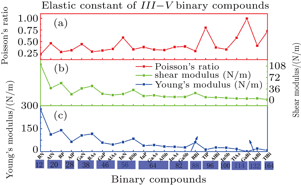
The Poisson’s ratio, shear modulus, and Young’s modulus as a function of relative radius are illustrated in Fig. 3. Note that TlN and TlSb with a negative Young’s modulus are excluded from the plot. As shown from Fig. 3, the shear modulus and Young’s modulus have a total decreasing trend with the increase of the relative radius, whereas the Poisson’s ratio is more complicated. However, it is interesting that all three mechanical constants will have a relatively big change at the boundary of different radius, e.g., from 28 to 38, 38 to 46, 46 to 56, 56 to 64, 82 to 88, 88 to 96, 96 to 100, and 114 to 132, and each of the elastic natures of different binary compounds with the same radius almost keep a relatively stable value (e.g., see the region denoted by blue rectangle). As seen from Fig. 3, BN has the largest shear and Young’s modulus in all III–V binary monolayer compounds due to its smallest radius. From this point we can speculate that some structures formed by B, C, and N elements with a close relative radius will be beneficial to the improvement of the mechanical property, such as borophene grown successfully on Ag (111) surface due to its extraordinary anisotropic mechanical properties.[24] The results[42] show that C3 N monolayer can withstand up to strain level of 12% for zigzag and armchair uniaxial strain and 10% for ab biaxial strain. Li found that B8 C12 is a new stable structure and is expected to be synthesized experimentally by using first-principles calculations.[43] Finally, it is worth noting that under a given relative radius, the binary compounds with a boron element show a slightly bigger shear and Young’s modulus than those of other binary compounds with the same radius, e.g., BP under radius=20, BAs under radius=38, BSb under radius=56, and BBi under radius=88, which validates the speculation above. Whether these binary compounds located in a symmetric region in Table 3 have any other similar properties is left for future study.
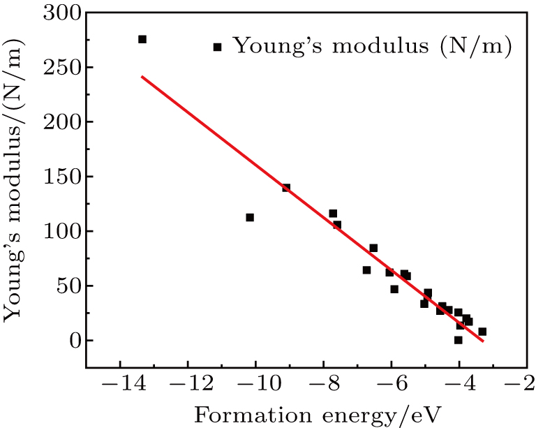
By analyzing the results of formation energy and Young’s modulus for all 25 kinds of binary compounds in III–V, we find an approximate linear relationship between the two physical quantities, and it is fitted to the following formula
where
Y and
E are the Young’s modulus and formation energy respectively. The Young’s modulus as a function of formation energy is shown in Fig.
4.
3.3. Electrical propertiesAfter analyzing the mechanical properties of those 25 kinds of III–V binary monolayer compounds, we start to investigate the electronic properties. We calculate the band structures, density of states, and band edge carrier effective mass for all III–V binary monolayer compounds respectively under uniaxial, equi-biaxial strained, and free-strained conditions at the PBE level. Since the band gaps of semiconductors are often underestimated by the standard density functional theory (DFT), the band structures of 25 kinds of binary compounds without strain are calculated by using the Heyd–Scuseria–Ernzerhof (HSE06) hybrid functional[34,44–47] for more rigorous scrutiny, during all calculations the screening parameter and the Hartree–Fock (HF) mixing parameter are chosen to be
 and α = 25% respectively. The band gaps calculated with the PBE and HSE06 levels, effective mass of the electron at the conduction band minimum (CBM) and the hole at the valence band maximum (VBM) are listed in Table 1, and the band gap types listed in Table 1 are denoted as D for a direct gap and ID for an indirect one, respectively. We note that the effective mass of carrier is calculated using PBE only by trading off the calculation time. More importantly, the shape of the band structure from PBE always changes a little compared with that of HSE06, and the effective mass is mainly determined by the shape of the band structure rather than the band gap by using a parabola fitting method.[23] As seen from Table 1, the band gap values of GaN, GaP, GaAs, and GaSb with PBE are 2.16, 1.64, 1.05, and 0.84 eV respectively, which are in agreement with those in Ref. [20], where the corresponding band gap values are 1.85, 1.56, 1.31, and 0.79 eV respectively. The underestimated band gaps are improved by the HSE06 method as shown in Table 1. The band gap of GaN calculated by HSE06 is 3.43 eV, which is very close to the experimental value 3.50 eV, and the experimental values of effective mass of the electron and hole are 0.18 and 1.64m0, which are also in agreement with the average values of our results.[23] However, the band gap of InN of a monolayer is 1.61 eV (HSE06) and is much larger than the experimental value (0.70 eV) in a bulk InN material. Our results for band gap values for GaAs, GaSb, InAs, and InSb monolayer structures are shown to be 1.85, 1.51, 1.44, and 1.32 eV respectively, which are larger than those of a zinc blende bulk phase structure with band gap values of 1.519, 0.822, 0.417, and 0.235 eV respectively.[1] The band gap of AlSb of our calculation is 1.97 eV, which is closed to the value in Ref. [38] with the same structure and GW0 method, but it is much smaller than 2.386 eV in Ref. [1], where the authors used a multi-band
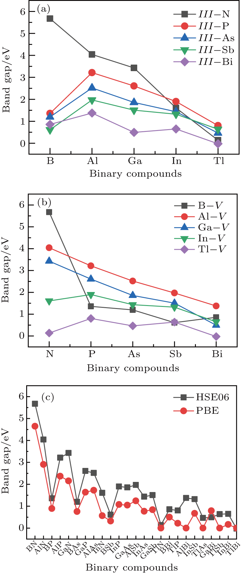
 method with a bulk structure. Other results of band gaps in our calculations are shown to be a little smaller than those in Ref. [38], where a more accurate method (GW0) was used but the variation trends are similar; thus we can use the data to conclude some regularity of electronic properties for the 25 kinds of binary compounds. It seems that the mechanical properties are quite radius dependent based on the analysis above. However, the band gaps have a similar trend when we intend to sort the band gaps according to the binary relative radii (not shown here). It is interesting that a new regularity exists in Table 1 for the band gaps; i.e., if we ignore the B–V (V = N, P, As, Sb, Bi) except for BN and for a given V-column element, all band gaps will decrease monotonically with the increase of III-element row number in the periodic table (see Fig. 5 (a)). Conversely, for a given III-column element, a similar regularity is found except for Tl–V (V = N, P, As, Sb, Bi) and InN (see Fig. 5(b)). Figure 5(c) shows the relation between the band gap and relative radius (defined above). It is interesting that the band gaps monotonically decrease with the increase of relative radius, accompanied by periodic fluctuations, and the regularity in Fig. 5(c) is not the same as that in Fig. 3 although the y-axial values in both plots decrease monotonically in the overall trend. One can find in Fig. 5(c) that the valleys of all periodic fluctuations are always located at very special points, e.g. at BP (20), BAs (38), BSb (56), TlN (88), TlAs (114), and TlBi (164), among which the first three binary compounds are finally located at the positions with the same relative radius in the 25 compounds, while the last three are located at first at the positions with the same relative radius in the latter half of the 25 compounds (see Table 3). According to Fig. 5, it can be concluded that the band gaps for III–V binary compounds are group, period and radius dependent.
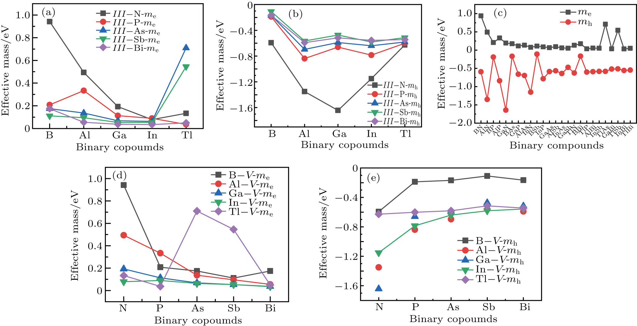
The plots of effective mass of carrier versus different binary compounds are depicted in Figs. 6(a) and 6(b) for the effective mass of the electron and hole under a given V element and different III elements, respectively; the plots of effective mass of both carriers versus all III–V binary compounds under a radius sorted case are exhibited in Fig. 6(c); the plots of effective mass of carrier versus different binary compounds are shown in Figs. 6(d) and 6(e) for the effective mass of the electron and hole under a given V element and different III elements, respectively. We note that each effective mass in Fig. 6 is averaged by the two K-path directions at CBM or VBM in Table 1. As seen from Fig. 6(c), the effective mass values of the electron for most III–V binary compounds are very close to 0.25m0; a number of exceptions are found in a very small or very large radius region, while the effective mass of the hole is seen to be more sensitive before BSb and followed by a relative stable value close to
 . One can find in Fig. 6(c) that a III–N binary will increase and a B–V binary will reduce the effective mass of the hole (AlN, BAs, etc.); i.e. almost all fluctuations of mh are found to be at either a III–N or a B–V binary, which can be seen more clearly in Figs. 6(b) and 6(e). By investigating Figs. 6(a) and 6(d), the effective mass of the electron of III–N and Tl–V are more sensitive with the increase of row numbers in the periodic table under a given N and Tl element respectively.
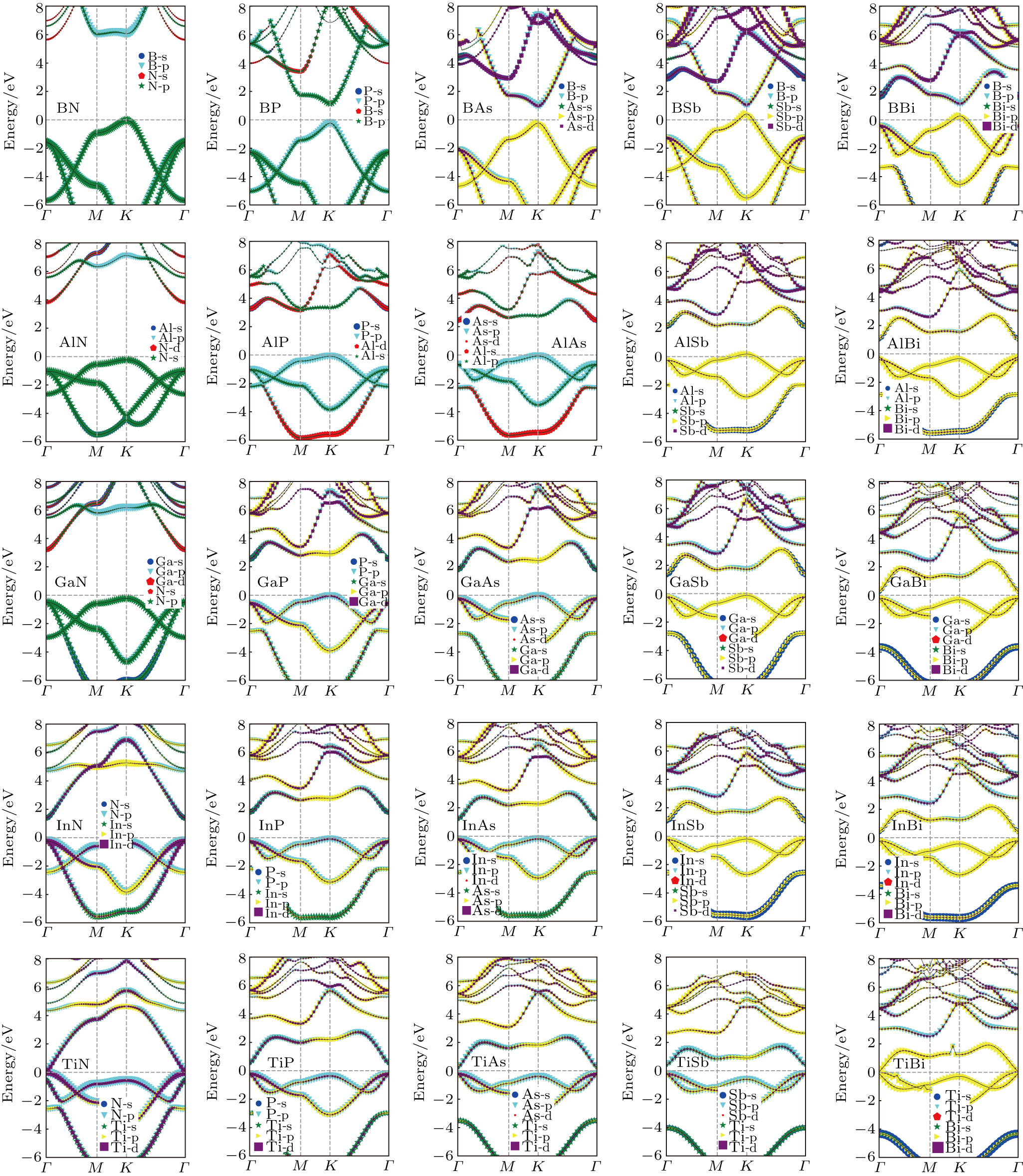
We further calculate the band structures of 25 kinds of III–V binary monolayer compounds subjected to no strain with the HSE06 method as shown in Fig. 7. It follows from Fig. 7 that all bands are projected into s, p, and d orbitals for a clear investigation about the contributions of electrons. By analyzing the band structures of all the considered binary monolayer compounds, we find that there are 14 kinds of direct bands, 10 kinds of indirect bands and 1 kind of metal band. A most obvious regularity in Fig. 7 is that the binary monolayer compounds located in the top and left have a larger gap while the bottom and right ones have a smaller gap, which shows intuitive information for experimental researchers who intend to synthesize a new material with given band gaps based on III–V elements. It can be found in Fig. 7 that the shape of an III–N binary is much different from those of other III–V binaries in the same row; we infer from this point that an N element will dominate the band structure and hence the electronic properties for a give III element. Interestingly, a similar regularity is found in the case of B–V binaries; i.e., for a given V element in the same column, the shape of band structure of B–V is very different from those of other compounds. The VBM is found to be contributed by V-p electrons for all structures, while the CBM is more sophisticated. For instance, the CBM of BN is mainly contributed by N-s electrons while the CBM of GaN is mainly contributed by both Ga-s and N-s electrons. Another regularity found in Fig. 7 is that the conduction bands of the former 20 kinds of III–V binaries tend to shift downward to reduce the gaps while the remaining 5 kinds of III–V binary compounds located in the fifth row keep fixed relatively.
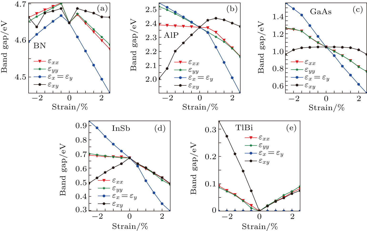
To investigate the effects of strain in different directions on the band properties of III–V monolayer structures, we calculate the uniaxial, equi-biaxial and shear strained band structures of all 25 kinds of III–V binary compounds at the PBE level rather than the HSE06 level. In this way we think it will be enough for us to investigate the change trend of the band structures in the case of strain. The most important reason for choosing a PBE level is that it consumes too much time for using a HSE06 level to calculate all 25 kinds of binaries and 44 times for each one. For simplicity, we choose only 5 binaries, but all 10 elements are included as an example to show the regularity of the gaps under strain conditions in different directions; the results are shown in Fig. 8. It can be found in Fig. 8 that the band gaps are very dependent on the strain in different directions, and the anisotropic property in the band gap of AlP is in agreement with that of strain energy in Fig. 2(b); the band gaps of AlP and InSb versus equi-biaxial strain are seen to have a similar change trend while the band gap of GaAs decreases with a constant slope. The band gap of BN decreases either under a compressed or under a tensile equi-biaxial strain, and in the case of TlBi the band gap is not affected by the equi-biaxial strain. Analyzing the other 20 kinds of III–V binary compounds (not shown here), we find that there is generally not regularity on the whole, so we will not give more detailed discussion about Fig. 8., However, it is worth noting that by using the strains in different directions, one can tune the gaps of III–V binary monolayers very flexibly.
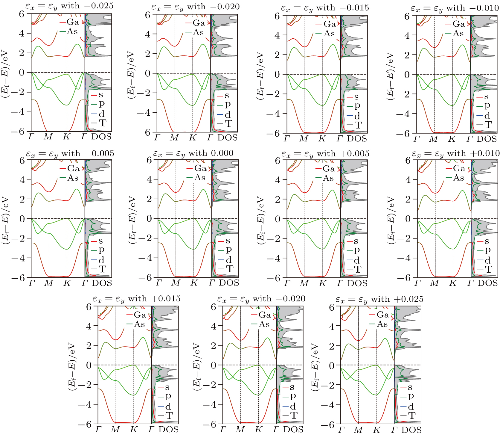
In order to show how the equi-biaxial strain can affect the band structure of a III–V binary compound, we take GaAs for example and the projected band structures and density of states of GaAs subjected to an equi-biaxial strain from −0.025 to 0.025, illustrated in Fig. 9. The results are in agreement with those in [20]. It can be found that the shape of band structure of GaAs at the PBE level is the same as that at the HSE06 level in Fig. 7, which proves that our calculations at the PBE level are accurate enough in the case where we just want to discuss the trends of band structures under different strains. From Fig. 9, one can find that a compress strain will shift the VBM to a lower location and the CBM to a higher location, which means that the band gap increases and agrees with the results in Fig. 8. In the case of a tensile strain, it is a little different; i.e., the VBM almost keeps fixed and the CBM is shifted to a lower location which leads the gap to decrease. From the partial density of states, we can know that the contribution of each orbital is nearly unaffected by the strain; i.e. under all different strains, the VBM is contributed by As(p) electrons and the CBM is contributed by Ga-s, As-s, and As-p electrons. It is worth noting that the equi-strain is able to not only shift the energy of CBM or VBM, but also change the type of band gap; e.g., GaAs under no strain seems to be an indirect gap semiconductor and gradually changes into a direct band gap semiconductor under a −0.025 equi-strain. Similar results are found in the other 24 kinds of compounds but are not shown here for simplicity.


