Direct observation of the f–c hybridization in the ordered uranium films on W(110)
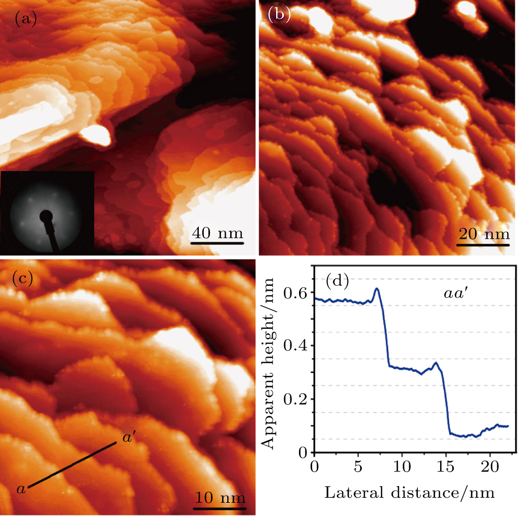
(a)–(c) STM images of the freshly deposited U films on the W(110) substrate after annealing at 800 K for 5 min with the sizes of (a) 200 nm ×200 nm, (b) 100 nm×100 nm, and (c) 50 nm×50 nm. The inset in panel (a) is LEED pattern of the ordered U films. (d) Line profile of
