† Corresponding author. E-mail:
Tin monoxide (SnO) is an interesting two-dimensional material because it is a rare oxide semiconductor with bipolar conductivity. However, the lower room temperature mobility limits the applications of SnO in the future. Thus, we systematically investigate the effects of different layer structures and strains on the electron–phonon coupling and phonon-limited mobility of SnO. The A2u phonon mode in the high-frequency region is the main contributor to the coupling with electrons for different layer structures. Moreover, the orbital hybridization of Sn atoms existing only in the bilayer structure changes the conduction band edge and conspicuously decreases the electron–phonon coupling, and thus the electronic transport performance of the bilayer is superior to that of other layers. In addition, the compressive strain of ε = −1.0% in the monolayer structure results in a conduction band minimum (CBM) consisting of two valleys at the Γ point and along the M–Γ line, and also leads to the intervalley electronic scattering assisted by the 

It is well known that dimension plays one of the crucial roles in the properties of materials because the dimensionality reduction can give rise to significant changes. Thus, since the discovery of graphene, we have witnessed an explosion of interest in developing two-dimensional (2D) materials and understanding their properties.[1,2] A common characteristic of 2D materials is the weak van der Waals interaction between the layers and strong bonding within the layers. Beyond the graphene, 2D materials, such as Xenes,[3–5] metal chalcogenides,[6–8] MXenes,[9,10] layered oxide materials,[11,12] and others,[13–16] have received considerable attention. The most monumental reason for this is that many motivating properties only exist in 2D materials. For example, the suitable bandgap, ultrahigh carrier mobility, and other novel quantum effects make them suitable for use in electronic, optical, and logic devices.[17–20]
Among the 2D materials, IV–VI compounds provide an opportunity for sustainable electronic and photonic systems due to their various structures, abundance in the earth, and nontoxic characteristics.[8,21] The ultrathin IV–VI compounds (SnS,[22–25] SnSe,[26,27] and SnSSe[28]) have been mechanically exfoliated and applied in high-performance field effect transistors. In addition, IV–VI compounds have demonstrated many interesting physical properties that are worthy of in-depth study.[29] For example, the direct bandgap of ∼1.5 eV makes SnS have a high absorption coefficient, and a promising candidate for solar cells, photodetectors, and photocatalytic water splitting.[30–32] The transformation from the amorphous to the crystalline state of SnSe under a laser showed its advantage over memory devices.[33–35] Theoretical work also predicted that SnSe has a layer-dependent bandgap and can transit from an indirect to a direct bandgap semiconductor when the thickness decreases to a monolayer, thus indicating its potential applications in optical and optoelectronic devices.[36] Furthermore, multiferroics,[37,38] piezoelectric,[39,40] and topological insulators[41–43] have also been predicted in the family of IV–VI compounds, greatly extending their future applications.
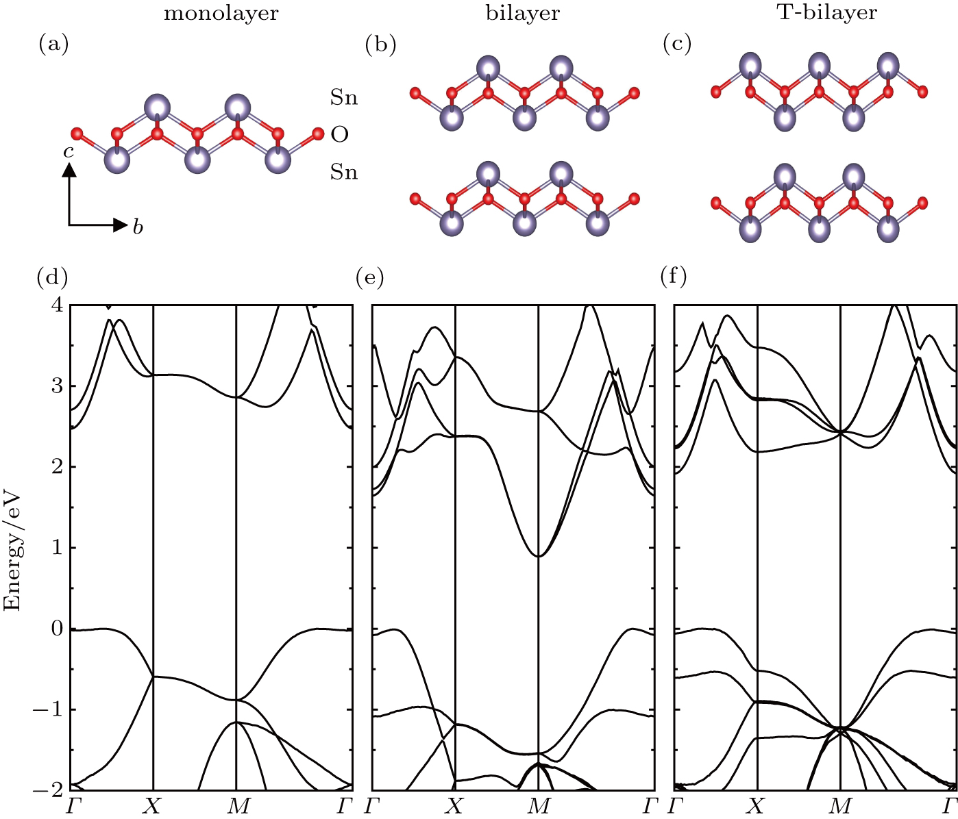
Tin monoxide (SnO) is an interesting semiconductor and shows promise for a wide variety of technological applications.[44] The stable phase of SnO has a tetragonal crystallographic structure (P4/nmm space group[45–47]). The specific lone pair[48] of 5s electrons in SnO leads to the dipole–dipole interaction and the unique structure versus other IV–VI compounds, which makes SnO a rare oxide semiconductor with bipolar conductivity.[49–51] The van der Waals interaction along the [001] crystal direction also makes SnO form a layered structure with the Sn–O–Sn sequence,[52–54] as shown in Fig. 
In experiments, several kinds of preparation methods[67] can control the production of high-quality 2D materials with a selected number of layers. It is found that many physical properties, especially the band edge structure, depend strongly on the number of layers. The twist angle between adjacent layers[68–71] can also affect electron structure. Moreover, strain engineering[72] has been successfully used to tailor the properties of 2D materials,[73–76] such as the crystal structure, bandgap, phonon, and so on. In order to study the effects of the above experimental methods on the electronic transport in SnO and provide the necessary calculation basis for the multifunctional applications of SnO, here, we study the electron–phonon coupling and phonon-limited mobility[77,78] of SnO modulated by different layer structures and strains based on first-principles calculations with Boltzmann transport theory. It is found that the A2u phonon mode in the high-frequency region contributes to the major electron–phonon coupling for different layer structures. It is noteworthy that the significant change in the conduction band edge of the bilayer results in a huge reduction of electron–phonon coupling, thus improving the electronic transport performance. In the monolayer structure, although the compressive strain of ε = −1.0% greatly impacts the conduction band edge and changes the region of the main electron–phonon coupling in the phonon spectrum, its comprehensive effect on the mobility is minimal when the other strains also have little effect on the electronic transport.
Our calculation is based on the semiclassical Boltzmann transport theory. The transport electron–phonon coupling constant λtr can be obtained by
 |

 |
 |

The technical details of the calculations are as follows. All calculations, including the electronic structures, the phonon spectra, and the electron–phonon couplings, were carried out using the ABINIT package[80–83] with the local-density approximation. The ion and electron interactions were treated with the Hartwigsen–Goedecker–Hutter pseudopotentials.[84] The strain was introduced by adjusting the lattice constant a of the monolayer SnO with the strain capacity 

The monolayer SnO consists of three atomic layers, with the oxygen layer sandwiched between two tin layers (Fig.
Furthermore, the number of layers and stacking types are also considered in the present work. First, the prototypical bilayer structure (denoted by bilayer for simplicity) is similar to the bulk structure (P4/nmm) but has a vacuum layer of 16 Å in order to be a 2D structure (Fig.
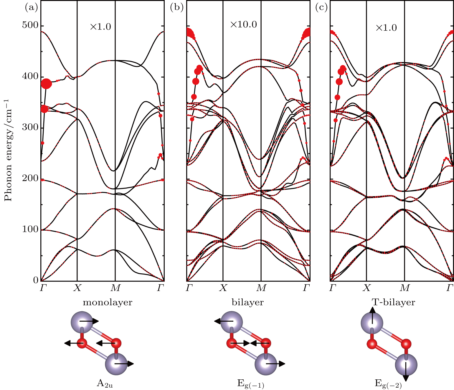
By using the DFPT, we calculated the phonon spectra and the electron–phonon couplings of the monolayer, bilayer, and T-bilayer. As shown in Fig. 


As shown in Fig. 
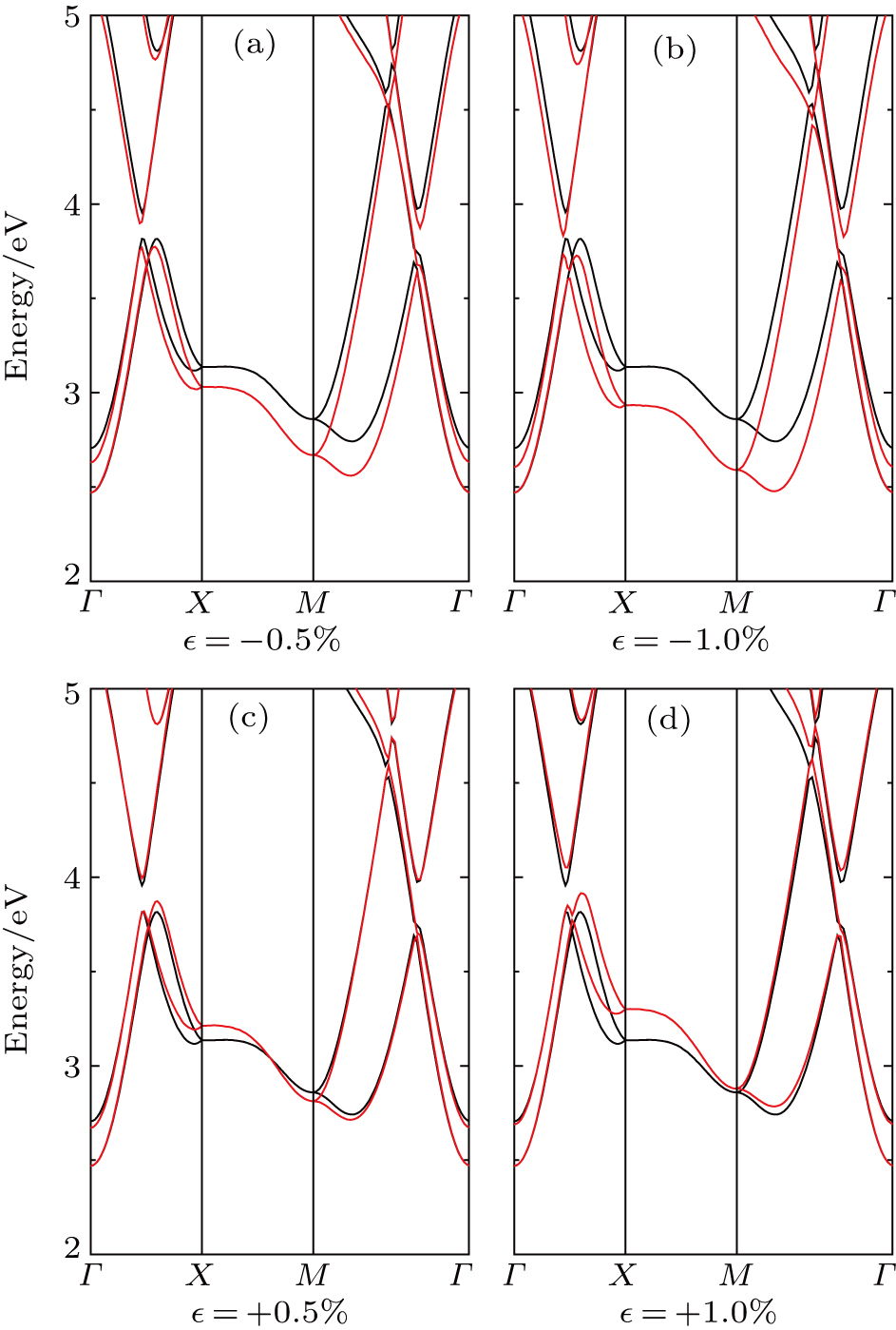
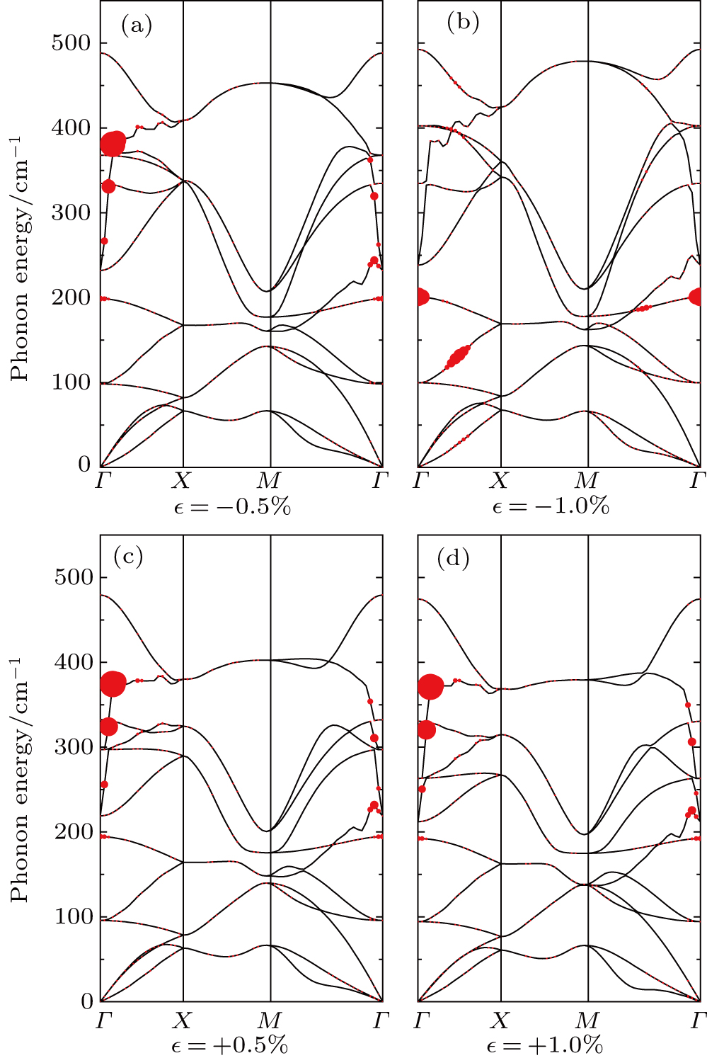
In addition to the effects of the number of layers and stacking types, we also study the influences of different extents and types of strains in the monolayer structure, including tensile and compressive strains. To ensure the dynamic stability of lattice structures, only strains of no more than 1% are considered in the present work, which will be discussed later. Under compressive strains, the conduction bands around points X and M are gradually approaching the CBM with the increase in strain, as shown in Fig.
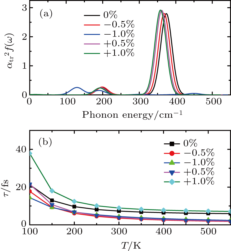
In the phonon spectra of different extents and types of strains (Fig. 


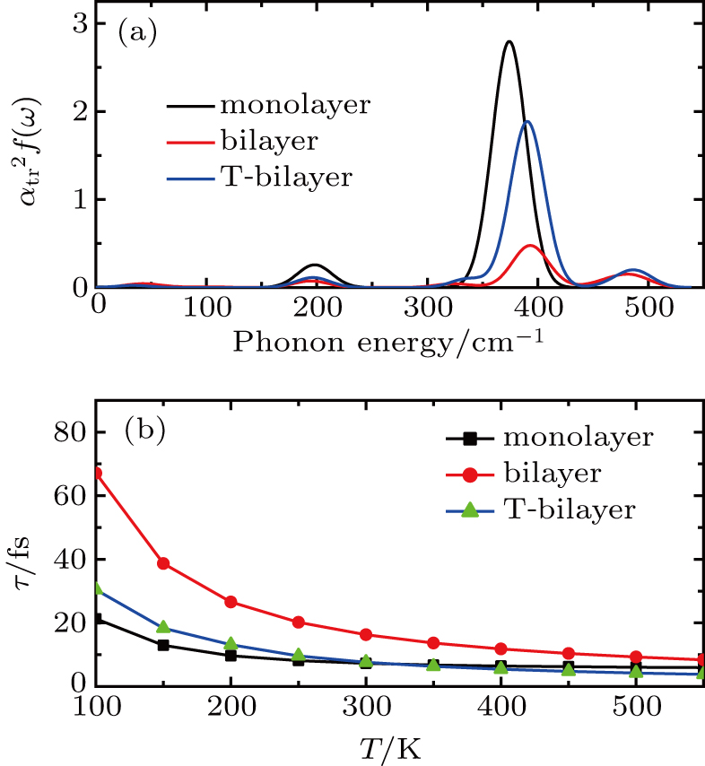
The transport spectral function 

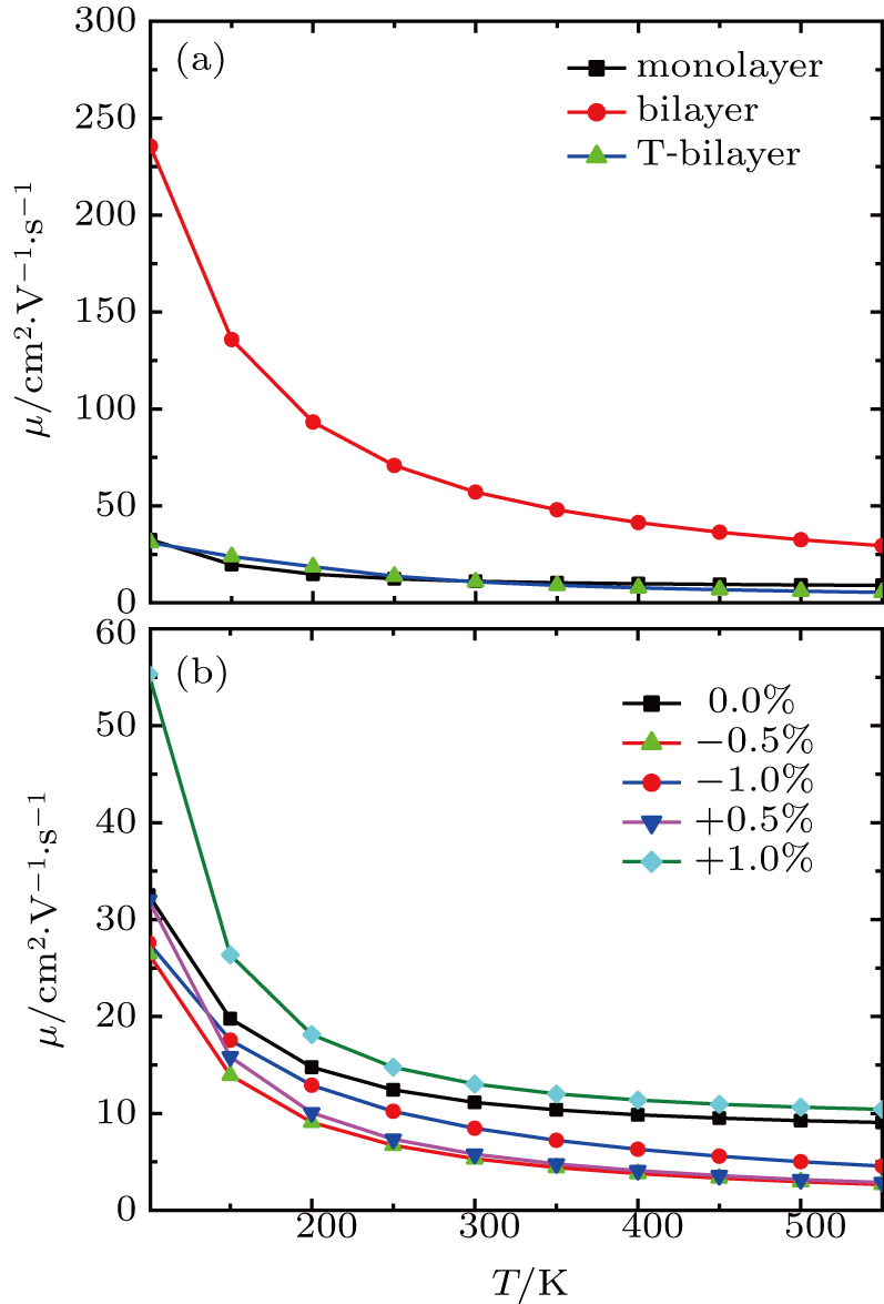
The carrier mobility μ as a function of the temperature for the structures with different layers and various strains is plotted in Fig. 


In summary, we have studied the effect of the number of layers and strains on the phonon-limited mobility of SnO. In the strain-free condition, it is found that the coupling of the electron with the A2u phonon mode in the high-frequency region is the strongest for the three types of layer structures. Furthermore, the interaction between Sn atoms from different layers in the bilayer structure obviously changes the CBM. Hence, the bilayer has the highest mobility of the three cases. After the introduction of strain in the monolayer structure, the compressive strain of ε = −1.0% leads to the CBM consisting of two valleys: one at the 


| [1] | |
| [2] | |
| [3] | |
| [4] | |
| [5] | |
| [6] | |
| [7] | |
| [8] | |
| [9] | |
| [10] | |
| [11] | |
| [12] | |
| [13] | |
| [14] | |
| [15] | |
| [16] | |
| [17] | |
| [18] | |
| [19] | |
| [20] | |
| [21] | |
| [22] | |
| [23] | |
| [24] | |
| [25] | |
| [26] | |
| [27] | |
| [28] | |
| [29] | |
| [30] | |
| [31] | |
| [32] | |
| [33] | |
| [34] | |
| [35] | |
| [36] | |
| [37] | |
| [38] | |
| [39] | |
| [40] | |
| [41] | |
| [42] | |
| [43] | |
| [44] | |
| [45] | |
| [46] | |
| [47] | |
| [48] | |
| [49] | |
| [50] | |
| [51] | |
| [52] | |
| [53] | |
| [54] | |
| [55] | |
| [56] | |
| [57] | |
| [58] | |
| [59] | |
| [60] | |
| [61] | |
| [62] | |
| [63] | |
| [64] | |
| [65] | |
| [66] | |
| [67] | |
| [68] | |
| [69] | |
| [70] | |
| [71] | |
| [72] | |
| [73] | |
| [74] | |
| [75] | |
| [76] | |
| [77] | |
| [78] | |
| [79] | |
| [80] | |
| [81] | |
| [82] | |
| [83] | |
| [84] | |
| [85] |


