Effects of helium irradiation dose and temperature on the damage evolution of Ti3SiC2 ceramic
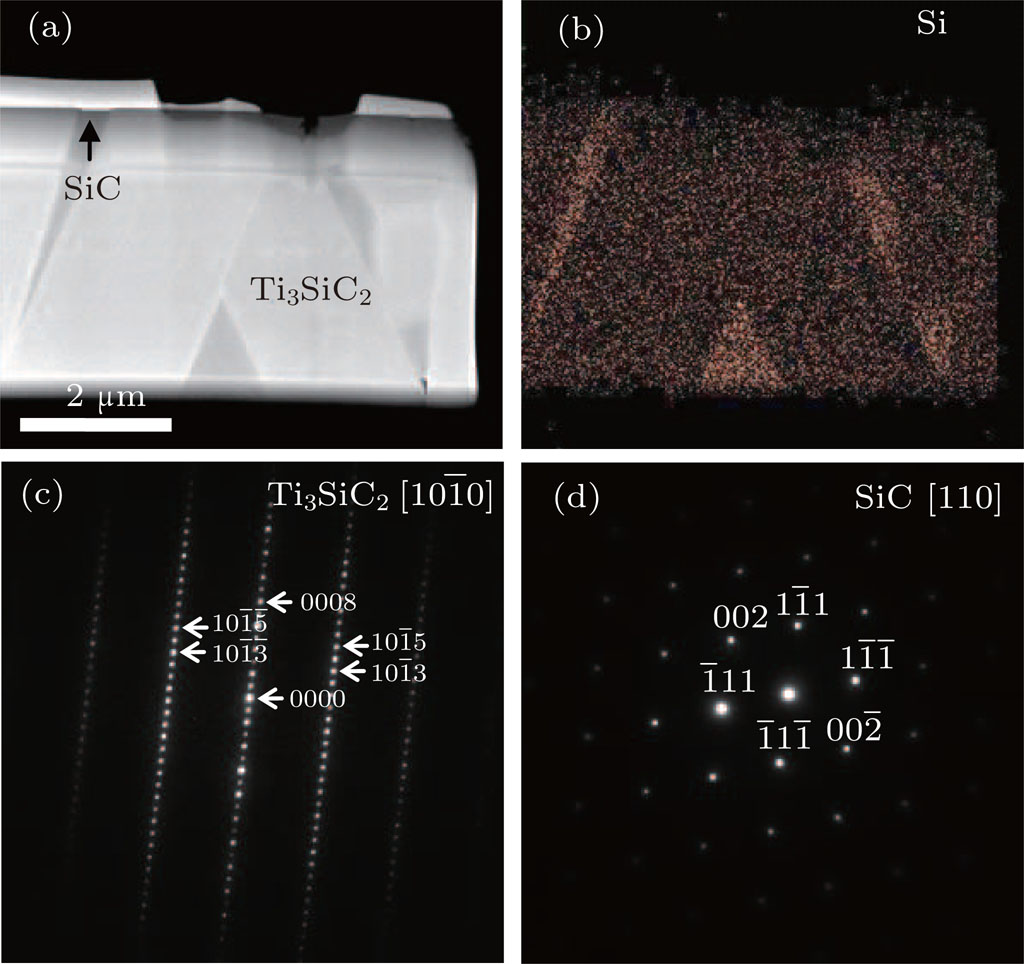
(a) STEM-ADF image of a Ti3SiC2 TEM specimen prepared by FIB method cutting across grain boundaries of Ti3SiC2 and impurity phases. (b) EDS mapping of Si element of the area shown in (a). (c) and (d) SAED patterns taken from the Ti3SiC2 and impurity phase grains along the viewing directions of [10
